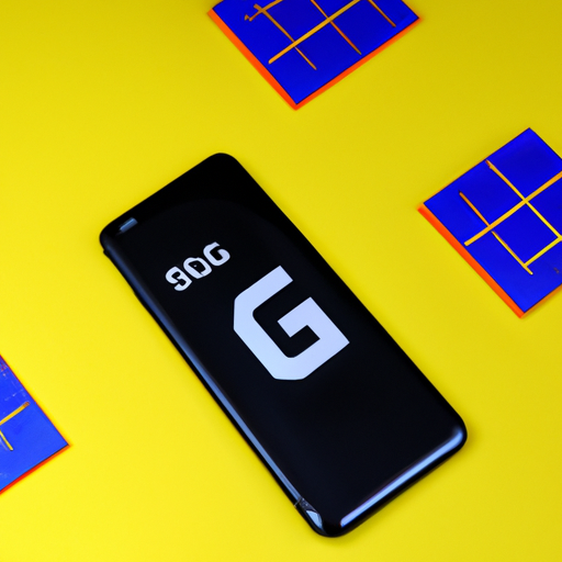
NEW
Popular Models of 5G Timing Modules
I. Introduction
As the world transitions into the era of 5G technology, the demand for precise timing solutions has never been more critical. **5G Timing Modules** are specialized devices that ensure synchronization across various components of a 5G network, enabling seamless communication and optimal performance. The importance of timing in 5G networks cannot be overstated; it directly impacts everything from data transfer rates to network reliability. This article will explore the popular models of 5G timing modules, their features, and their applications, providing a comprehensive overview for those interested in this essential technology.
II. Understanding 5G Timing Requirements
A. The Role of Timing in 5G Networks
Timing plays a pivotal role in the functioning of 5G networks. With the introduction of ultra-reliable low-latency communication (URLLC) and massive machine-type communication (mMTC), the need for precise synchronization has become paramount.
1. Synchronization Needs
In a 5G network, various components such as base stations, user equipment, and core network elements must operate in perfect harmony. This synchronization is crucial for maintaining the integrity of data transmission and ensuring that signals are sent and received without delay.
2. Impact on Network Performance
Poor timing can lead to increased latency, reduced throughput, and even network failures. Therefore, 5G timing modules are designed to meet stringent timing requirements, ensuring that networks can deliver the high performance expected from 5G technology.
B. Key Timing Standards and Protocols
To achieve the necessary synchronization, several key standards and protocols are employed:
1. ITU-T Recommendations
The International Telecommunication Union (ITU) provides recommendations that guide the implementation of timing solutions in telecommunications. These recommendations help ensure that timing modules meet global standards.
2. IEEE 1588 Precision Time Protocol (PTP)
IEEE 1588, also known as PTP, is a protocol used for precise clock synchronization in networked systems. It is particularly important in 5G networks, where microsecond-level accuracy is often required.
3. Network Time Protocol (NTP)
NTP is another widely used protocol for synchronizing clocks over packet-switched networks. While it is less precise than PTP, it is still essential for many applications within 5G networks.
III. Popular Models of 5G Timing Modules
A. Overview of Leading Manufacturers
Several manufacturers are at the forefront of developing 5G timing modules. These include:
1. **Keysight Technologies**
2. **Microchip Technology**
3. **Analog Devices**
4. **u-blox**
5. **NXP Semiconductors**
B. Detailed Analysis of Popular Models
1. Keysight Technologies
**Model: M8195A**
Features and Specifications: The M8195A is a high-performance arbitrary waveform generator that supports 5G NR (New Radio) testing. It offers a frequency range of up to 6 GHz and can generate complex waveforms with high fidelity.
Applications and Use Cases: This model is ideal for testing 5G devices and networks, ensuring that they meet the required timing and performance standards.
2. Microchip Technology
**Model: MCP19111**
Features and Specifications: The MCP19111 is a versatile timing module that supports various timing protocols, including PTP and NTP. It features low power consumption and high accuracy, making it suitable for battery-operated devices.
Applications and Use Cases: This module is commonly used in IoT applications, where precise timing is essential for data collection and transmission.
3. Analog Devices
**Model: AD9548**
Features and Specifications: The AD9548 is a high-performance clock generator that supports multiple output frequencies and synchronization protocols. It is designed for applications requiring high stability and low jitter.
Applications and Use Cases: This model is widely used in telecommunications infrastructure, including base stations and routers.
4. u-blox
**Model: ZED-F9P**
Features and Specifications: The ZED-F9P is a high-precision GNSS receiver that provides accurate timing information. It supports multi-band GNSS signals and offers centimeter-level positioning accuracy.
Applications and Use Cases: This module is ideal for applications in autonomous vehicles and robotics, where precise timing and positioning are critical.
5. NXP Semiconductors
**Model: T1040**
Features and Specifications: The T1040 is a powerful timing module that integrates multiple timing protocols and offers high accuracy and stability. It is designed for use in complex network environments.
Applications and Use Cases: This model is commonly used in 5G base stations and other critical infrastructure components.
IV. Comparison of 5G Timing Modules
A. Performance Metrics
When evaluating 5G timing modules, several performance metrics should be considered:
1. Accuracy
Accuracy is crucial for ensuring that devices can communicate effectively. Modules like the AD9548 and ZED-F9P are known for their high accuracy, making them suitable for demanding applications.
2. Stability
Stability refers to the module's ability to maintain consistent performance over time. The MCP19111 and T1040 are recognized for their stability, which is essential for long-term deployments.
3. Environmental Resilience
5G timing modules must operate reliably in various environmental conditions. Models like the M8195A are designed to withstand harsh conditions, making them suitable for outdoor installations.
B. Cost Considerations
Cost is always a factor when selecting timing modules. While high-performance models may come with a higher price tag, the investment is often justified by the improved network performance and reliability they provide.
C. Integration and Compatibility with Existing Systems
Compatibility with existing systems is another critical consideration. Many manufacturers design their timing modules to be easily integrated into current network infrastructures, ensuring a smooth transition to 5G technology.
V. Future Trends in 5G Timing Modules
A. Technological Advancements
The future of 5G timing modules is likely to be shaped by several technological advancements:
1. Enhanced Precision and Accuracy
As 5G networks evolve, the demand for even greater precision and accuracy will grow. Manufacturers are already working on developing modules that can achieve sub-microsecond synchronization.
2. Miniaturization and Power Efficiency
There is a trend towards miniaturization, with manufacturers striving to create smaller, more efficient timing modules that consume less power. This is particularly important for IoT devices and other battery-operated applications.
B. The Role of AI and Machine Learning
Artificial intelligence and machine learning are expected to play a significant role in the future of 5G timing modules. These technologies can help optimize timing algorithms and improve synchronization accuracy.
C. Emerging Standards and Protocols
As 5G technology continues to evolve, new standards and protocols will emerge. Manufacturers will need to stay ahead of these developments to ensure their timing modules remain relevant and effective.
VI. Conclusion
In summary, 5G timing modules are essential components of modern telecommunications networks. They ensure synchronization, improve network performance, and enable the seamless operation of various applications. With numerous models available from leading manufacturers, it is crucial to choose the right timing module based on specific requirements and use cases. As technology advances, the future of 5G timing modules looks promising, with enhanced precision, miniaturization, and the integration of AI and machine learning on the horizon.
VII. References
- Academic Journals
- Industry Reports
- Manufacturer Specifications and White Papers
This comprehensive overview of popular models of 5G timing modules highlights their importance in the telecommunications landscape and provides insights into the future of this critical technology.
How to Choose the Off-the-Shelf 5G Transmission Module
I. Introduction
As we step into the era of 5G technology, the landscape of connectivity is evolving at an unprecedented pace. 5G, or fifth-generation wireless technology, promises to deliver faster speeds, lower latency, and the ability to connect a vast number of devices simultaneously. This transformation is not just limited to smartphones; it extends to various applications, including the Internet of Things (IoT), smart cities, autonomous vehicles, and more. At the heart of these advancements are 5G transmission modules, which play a crucial role in enabling devices to communicate over 5G networks.
This guide aims to assist you in selecting the right off-the-shelf 5G transmission module for your specific needs. With numerous options available in the market, understanding the key factors to consider can help you make an informed decision.
II. Understanding 5G Transmission Modules
A. Definition and Function of 5G Transmission Modules
A 5G transmission module is a hardware component that enables devices to connect to 5G networks. These modules facilitate the transmission and reception of data, allowing devices to communicate wirelessly. They are essential for any application that requires high-speed internet access and low latency.
B. Key Components of a 5G Transmission Module
1. **Antenna**: The antenna is responsible for sending and receiving radio signals. The design and quality of the antenna can significantly impact the module's performance.
2. **Modem**: The modem converts digital data into radio signals and vice versa. It is a critical component that determines the module's data processing capabilities.
3. **RF Components**: Radio Frequency (RF) components manage the transmission and reception of signals. These components include filters, amplifiers, and mixers, which are vital for ensuring signal integrity.
C. Types of 5G Transmission Modules
1. **Embedded Modules**: These are integrated directly into devices, providing a compact solution for manufacturers. They are ideal for IoT applications where space is limited.
2. **External Modules**: These modules connect to devices via USB or other interfaces. They offer flexibility and can be easily replaced or upgraded.
3. **USB Dongles**: USB dongles are portable devices that provide 5G connectivity to laptops and other devices. They are user-friendly and ideal for temporary or mobile use.
III. Key Factors to Consider When Choosing a 5G Transmission Module
A. Application Requirements
Understanding your application requirements is the first step in selecting a 5G transmission module. Consider the following:
1. **Use Case Scenarios**: Different applications have varying needs. For instance, IoT devices may require low power consumption and long-range connectivity, while mobile broadband applications may prioritize high data rates.
2. **Data Rate and Bandwidth Needs**: Assess the amount of data your application will transmit. Higher data rates are essential for applications like video streaming, while lower rates may suffice for simple sensor data.
3. **Latency Requirements**: Some applications, such as autonomous driving, require ultra-low latency. Ensure the module you choose meets these requirements.
B. Compatibility
1. **Device Compatibility**: Ensure the module is compatible with your existing hardware and software. Check for supported interfaces and operating systems.
2. **Network Compatibility**: 5G networks operate on different frequency bands, primarily sub-6 GHz and mmWave. Verify that the module supports the frequency bands used by your network provider.
C. Performance Specifications
1. **Maximum Data Throughput**: Look for modules that offer high data throughput to meet your application's demands.
2. **Range and Coverage**: Evaluate the module's range and coverage capabilities, especially if your application requires connectivity in remote areas.
3. **Power Consumption**: For battery-operated devices, low power consumption is crucial. Compare the power requirements of different modules.
D. Regulatory Compliance
1. **Certification Requirements**: Ensure the module complies with relevant certifications, such as FCC (Federal Communications Commission) in the U.S. and CE (Conformité Européenne) in Europe.
2. **Frequency Band Regulations**: Different regions have specific regulations regarding frequency bands. Verify that the module adheres to these regulations.
E. Environmental Considerations
1. **Operating Temperature Range**: Consider the environmental conditions in which the module will operate. Ensure it can function within the required temperature range.
2. **Durability and Ruggedness**: For applications in harsh environments, choose modules that are rugged and can withstand physical stress.
F. Cost and Budget
1. **Initial Purchase Cost**: Compare the prices of different modules, keeping in mind that higher costs may be justified by better performance or features.
2. **Long-Term Operational Costs**: Consider ongoing costs, such as data plans and maintenance, when evaluating the total cost of ownership.
IV. Evaluating Manufacturer Reputation and Support
Choosing a reputable manufacturer is essential for ensuring the quality and reliability of your 5G transmission module. Research the manufacturer's track record, customer reviews, and industry reputation. Additionally, assess the level of customer support they offer, including warranty options and technical assistance. Availability of documentation and resources, such as user manuals and integration guides, is also crucial for a smooth implementation process.
V. Future-Proofing Your Choice
As technology continues to evolve, it is essential to consider future-proofing your investment. Look for modules that offer scalability and upgrade options, allowing you to adapt to changing requirements. Anticipate future technology trends, such as advancements in 5G standards and the emergence of 6G. Ensure that the manufacturer provides regular software updates and support to keep your module up to date.
VI. Case Studies and Examples
To illustrate the practical applications of 5G transmission modules, consider the following case studies:
1. **Healthcare**: In telemedicine, 5G transmission modules enable real-time video consultations between doctors and patients, improving access to healthcare services.
2. **Automotive**: Autonomous vehicles rely on 5G connectivity for real-time data exchange, enhancing safety and navigation capabilities.
3. **Smart Cities**: 5G modules facilitate the deployment of smart sensors and devices, enabling efficient traffic management and energy consumption monitoring.
These examples highlight the versatility and potential of 5G transmission modules across various industries.
VII. Conclusion
Choosing the right off-the-shelf 5G transmission module is a critical decision that can significantly impact the success of your application. By considering key factors such as application requirements, compatibility, performance specifications, and manufacturer reputation, you can make an informed choice. Conduct thorough research and evaluate your options to ensure that your selected module meets both current and future needs.
In the rapidly evolving world of technology, making an informed decision today can pave the way for successful implementations tomorrow.
VIII. Additional Resources
To further assist you in your research, consider exploring the following resources:
1. **Recommended Reading**: Look for books and articles on 5G technology and its applications.
2. **Websites**: Visit industry websites and blogs that focus on telecommunications and IoT.
3. **Industry Forums**: Join online communities and forums to discuss experiences and gather insights from other professionals.
4. **Expert Consultations**: Reach out to industry experts for personalized advice and recommendations.
By leveraging these resources, you can deepen your understanding of 5G transmission modules and make a well-informed decision for your specific needs.
The Role of Products Used in 5G Modules in Practical Applications
I. Introduction
The advent of 5G technology marks a significant leap in the evolution of mobile communication. Defined as the fifth generation of wireless technology, 5G promises to deliver faster speeds, lower latency, and the ability to connect a vast number of devices simultaneously. This transformative technology is not just about enhancing mobile broadband; it is set to revolutionize various sectors, including healthcare, transportation, and entertainment. At the heart of this innovation are the products used in 5G modules, which play a crucial role in enabling the practical applications of 5G technology. This blog post will explore the components of 5G modules, the key products involved, their applications, challenges, and future trends.
II. Understanding 5G Modules
A. Definition and Components of 5G Modules
5G modules are essential components that facilitate the operation of 5G networks. They consist of several critical elements, including:
1. **Antennas**: These are responsible for transmitting and receiving radio signals. The design and configuration of antennas significantly impact the performance of 5G networks.
2. **RF (Radio Frequency) Components**: These components manage the radio signals, ensuring that they are transmitted and received effectively.
3. **Baseband Processors**: These processors handle the data processing tasks, including modulation and demodulation of signals.
4. **Power Amplifiers**: These are crucial for boosting the signal strength, ensuring that the transmitted signals can cover larger distances.
B. Types of 5G Modules
5G modules can be categorized into two main types:
1. **Integrated Modules**: These combine multiple components into a single unit, offering compactness and efficiency.
2. **Discrete Modules**: These consist of separate components that can be individually optimized for specific applications.
III. Key Products Used in 5G Modules
A. Antennas
Antennas are pivotal in 5G technology, particularly with the implementation of MIMO (Multiple Input Multiple Output) and beamforming techniques. MIMO technology allows multiple signals to be transmitted and received simultaneously, significantly enhancing data throughput. Beamforming directs the signal towards specific users rather than broadcasting it in all directions, improving signal quality and reducing interference.
B. RF Components
RF components, including filters, mixers, and amplifiers, are vital for maintaining signal integrity and quality. Filters eliminate unwanted frequencies, ensuring that only the desired signals are processed. Mixers combine different frequencies, which is essential for various communication protocols. Amplifiers boost the signal strength, which is crucial for maintaining quality over long distances.
C. Baseband Processors
Baseband processors are the brains of 5G modules, responsible for processing the data that is transmitted and received. They handle tasks such as modulation, which converts data into a format suitable for transmission, and demodulation, which reverses this process. The efficiency and speed of baseband processors directly impact the overall performance of 5G networks.
D. Power Amplifiers
Power amplifiers are essential for ensuring that signals can travel long distances without degradation. They increase the power of the transmitted signals, which is particularly important in urban environments where buildings and other structures can obstruct signals. Additionally, efficient thermal management in power amplifiers is crucial to prevent overheating and ensure reliable operation.
IV. Practical Applications of 5G Modules
A. Telecommunications
5G technology is set to enhance telecommunications significantly. With improved mobile broadband capabilities, users can expect faster download and upload speeds, enabling seamless streaming and communication. Fixed wireless access will also become more prevalent, providing high-speed internet to areas where traditional broadband is unavailable.
B. Internet of Things (IoT)
The Internet of Things (IoT) is one of the most promising applications of 5G technology. In smart cities, 5G enables the interconnectivity of various devices, from traffic lights to waste management systems, leading to improved efficiency and sustainability. In industrial automation, 5G facilitates real-time monitoring and control of machinery, enhancing productivity and safety.
C. Autonomous Vehicles
5G technology plays a crucial role in the development of autonomous vehicles. Vehicle-to-everything (V2X) communication allows vehicles to communicate with each other and with infrastructure, improving safety and efficiency. Real-time data transmission enables vehicles to make informed decisions, reducing the likelihood of accidents and traffic congestion.
D. Healthcare
In the healthcare sector, 5G technology enables remote monitoring and telemedicine services. Patients can be monitored in real-time, allowing for timely interventions and reducing the need for hospital visits. The high-speed data transmission capabilities of 5G also facilitate the sharing of large medical files, such as imaging scans, enhancing collaboration among healthcare professionals.
E. Entertainment and Media
5G technology is set to transform the entertainment and media landscape. With the ability to support augmented reality (AR) and virtual reality (VR) applications, users can experience immersive content like never before. Additionally, streaming services will benefit from faster speeds and lower latency, providing a seamless viewing experience for users.
V. Challenges and Considerations
A. Technical Challenges in 5G Module Deployment
Despite its potential, the deployment of 5G modules faces several technical challenges. Interference and signal degradation can occur due to environmental factors and the dense urban infrastructure. Additionally, the deployment of 5G requires significant infrastructure investments, including the installation of new antennas and base stations.
B. Economic Considerations
The cost of implementing 5G technology is another significant consideration. While the long-term benefits may outweigh the initial investments, businesses and governments must carefully evaluate the return on investment. The economic viability of 5G projects will depend on the successful integration of technology and the development of new business models.
C. Regulatory and Security Issues
Regulatory compliance is crucial for the successful deployment of 5G technology. Governments must establish standards to ensure the safety and reliability of 5G networks. Additionally, data privacy and security concerns must be addressed, as the increased connectivity of devices raises the risk of cyberattacks.
VI. Future Trends in 5G Technology
A. Evolution of 5G Modules
The future of 5G technology will likely see the evolution of 5G modules towards miniaturization and integration. Advanced materials and technologies will enable the development of smaller, more efficient components, enhancing the overall performance of 5G networks.
B. Potential Impact on Various Industries
The impact of 5G technology on various industries is expected to be profound. Predictions suggest significant growth and innovation in sectors such as healthcare, transportation, and entertainment. As 5G technology continues to evolve, it will play a crucial role in driving future technological advancements.
VII. Conclusion
In conclusion, the products used in 5G modules are fundamental to the successful implementation and operation of 5G technology. From antennas to power amplifiers, each component plays a vital role in enabling the practical applications of 5G across various sectors. As we move forward, the transformative potential of 5G technology will continue to shape our world, driving innovation and improving the quality of life. It is essential for stakeholders to invest in research and development to fully realize the benefits of this groundbreaking technology. The future of communication is here, and it is powered by 5G.
Popular 5G Module Picture Product Models
Introduction
The advent of 5G technology marks a significant leap in mobile connectivity, promising faster speeds, lower latency, and the ability to connect a vast number of devices simultaneously. As industries and consumers alike embrace this new era of connectivity, 5G modules play a crucial role in enabling devices to harness the full potential of 5G networks. This article aims to explore some of the most popular 5G module product models currently available in the market, highlighting their features, applications, and significance in the evolving landscape of wireless communication.
1. Understanding 5G Modules
1.1 Definition of 5G Modules
5G modules are compact hardware components that enable devices to connect to 5G networks. These modules integrate various technologies, including radio frequency (RF) components, baseband processors, and software, to facilitate high-speed data transmission. They are essential for a wide range of applications, from smartphones and tablets to IoT devices and industrial machinery.
1.2 Key Features of 5G Modules
The key features of 5G modules include:
Speed and Bandwidth Capabilities: 5G modules can deliver data rates exceeding 10 Gbps, significantly enhancing user experiences in applications such as streaming, gaming, and virtual reality.
Latency Improvements: With latency as low as 1 millisecond, 5G modules enable real-time communication, which is critical for applications like autonomous vehicles and remote surgery.
Compatibility with Existing Networks: Many 5G modules are designed to be backward compatible with 4G and 3G networks, ensuring seamless connectivity during the transition to 5G.
2. Market Overview of 5G Modules
2.1 Growth of the 5G Market
The 5G market has witnessed exponential growth since its inception, with global 5G subscriptions expected to reach over 1.5 billion by 2025. Industries such as telecommunications, automotive, healthcare, and manufacturing are driving the demand for 5G modules, as they seek to leverage the technology for enhanced operational efficiency and innovative applications.
2.2 Major Players in the 5G Module Market
Several key players dominate the 5G module market, including Qualcomm, MediaTek, Sierra Wireless, Telit, and u-blox. These manufacturers are continuously innovating and expanding their product offerings to meet the growing demand for 5G connectivity. A comparison of their market share reveals a competitive landscape, with each company bringing unique strengths to the table.
3. Popular 5G Module Product Models
3.1 Qualcomm Snapdragon X55
The Qualcomm Snapdragon X55 is one of the most widely recognized 5G modules, known for its robust performance and versatility.
Specifications and Features: It supports both standalone (SA) and non-standalone (NSA) modes, offering flexibility for network deployment. The X55 can achieve download speeds of up to 7 Gbps and upload speeds of 3 Gbps.
Use Cases and Applications: This module is ideal for smartphones, laptops, and IoT devices, enabling high-speed internet access and seamless connectivity.
Advantages and Limitations: The X55's advanced features make it a top choice for manufacturers, but its complexity may lead to higher integration costs.
3.2 MediaTek Dimensity 1000
The MediaTek Dimensity 1000 is another popular 5G module, particularly in the smartphone market.
Specifications and Features: It integrates a 5G modem with an octa-core CPU, supporting dual SIM 5G connectivity. The Dimensity 1000 can deliver speeds of up to 4 Gbps.
Use Cases and Applications: This module is primarily used in mid-range smartphones, providing users with 5G capabilities at a more affordable price point.
Advantages and Limitations: Its cost-effectiveness is a significant advantage, but it may not match the performance of higher-end modules like the Snapdragon X55.
3.3 Sierra Wireless AirPrime 5G
Sierra Wireless offers the AirPrime 5G module, designed for industrial and IoT applications.
Specifications and Features: The AirPrime 5G supports global 5G bands and features advanced security protocols, making it suitable for critical applications.
Use Cases and Applications: It is commonly used in smart cities, connected vehicles, and remote monitoring systems.
Advantages and Limitations: Its robust security features are a major plus, but the module may be more expensive than consumer-grade options.
3.4 Telit FN980
The Telit FN980 is a compact 5G module that caters to various IoT applications.
Specifications and Features: It supports both 5G and LTE networks, with a focus on low power consumption and small form factor.
Use Cases and Applications: The FN980 is ideal for smart meters, asset tracking, and industrial automation.
Advantages and Limitations: Its low power consumption is beneficial for battery-operated devices, but its performance may not be as high as other models.
3.5 u-blox TOBY-R5
The u-blox TOBY-R5 is a versatile 5G module designed for a wide range of applications.
Specifications and Features: It supports global 5G bands and offers a compact design, making it suitable for various devices.
Use Cases and Applications: The TOBY-R5 is used in automotive, industrial, and consumer applications, providing reliable connectivity.
Advantages and Limitations: Its versatility is a significant advantage, but it may lack some advanced features found in more specialized modules.
4. Comparison of 5G Module Product Models
4.1 Performance Metrics
When comparing the performance of these 5G modules, factors such as speed, latency, and reliability are crucial. The Qualcomm Snapdragon X55 generally leads in speed, while the MediaTek Dimensity 1000 offers a good balance of performance and cost. The Sierra Wireless AirPrime excels in reliability for industrial applications, while the Telit FN980 and u-blox TOBY-R5 provide solid performance for IoT use cases.
4.2 Cost Analysis
The price range of these modules varies significantly. The MediaTek Dimensity 1000 is often the most affordable option, making it attractive for mid-range devices. In contrast, the Qualcomm Snapdragon X55 and Sierra Wireless AirPrime tend to be on the higher end of the spectrum, reflecting their advanced features and capabilities.
4.3 Application Suitability
Each module has its strengths in specific applications. The Snapdragon X55 is ideal for high-end smartphones, while the Dimensity 1000 is well-suited for budget-friendly devices. The Sierra Wireless AirPrime is tailored for industrial applications, and the Telit FN980 and u-blox TOBY-R5 cater to IoT solutions.
5. Future Trends in 5G Modules
5.1 Technological Advancements
As 5G technology continues to evolve, we can expect significant advancements in 5G modules. Emerging technologies such as integrated AI capabilities, enhanced security features, and improved energy efficiency are likely to shape the next generation of 5G modules.
5.2 Market Trends
The 5G module market is expected to grow rapidly, driven by increasing demand for IoT devices and smart applications. However, challenges such as regulatory hurdles and the need for infrastructure investment may impact growth. Opportunities lie in sectors like healthcare, automotive, and smart cities, where 5G can enable transformative solutions.
Conclusion
5G modules are at the forefront of the connectivity revolution, enabling a wide range of applications across various industries. The popular product models discussed in this article, including the Qualcomm Snapdragon X55, MediaTek Dimensity 1000, Sierra Wireless AirPrime, Telit FN980, and u-blox TOBY-R5, each offer unique features and capabilities that cater to different market needs. As we look to the future, the continued evolution of 5G technology and modules will undoubtedly play a pivotal role in shaping the way we connect and interact with the world around us.
References
- [5G Technology Overview](https://www.5gtechnology.com)
- [Market Analysis of 5G Modules](https://www.5gmarketanalysis.com)
- [Qualcomm Snapdragon X55 Specifications](https://www.qualcomm.com/products/snapdragon-x55)
- [MediaTek Dimensity 1000 Features](https://www.mediatek.com/products/dimensity-1000)
- [Sierra Wireless AirPrime 5G](https://www.sierrawireless.com/products/airprime-5g)
- [Telit FN980 Overview](https://www.telit.com/products/fn980)
- [u-blox TOBY-R5 Specifications](https://www.u-blox.com/en/product/toby-r5)

Understanding 5G Terminal Modules
I. Introduction
As we stand on the brink of a new era in communication technology, the term "5G terminal module" is becoming increasingly prevalent. But what exactly is a 5G terminal module, and why is it important? In simple terms, a 5G terminal module is a device that enables communication over 5G networks, facilitating faster data transfer, lower latency, and enhanced connectivity. The significance of 5G technology in modern communication cannot be overstated; it promises to revolutionize industries, enhance user experiences, and pave the way for innovations that were once thought to be the stuff of science fiction. This article aims to educate readers about 5G terminal modules, their components, functionality, applications, and the challenges they face.
II. Overview of 5G Technology
A. Evolution of Mobile Networks
To understand 5G terminal modules, it’s essential to grasp the evolution of mobile networks. The journey began with 1G, which introduced analog voice communication. This was followed by 2G, which brought digital voice and SMS capabilities. The advent of 3G enabled mobile internet access, while 4G significantly improved data speeds and introduced mobile broadband. Now, with 5G, we are witnessing a transformative leap that enhances not just speed but also connectivity and responsiveness.
B. Key Features of 5G Technology
5G technology is characterized by several key features:
1. **Enhanced Data Speeds**: 5G networks can deliver data speeds up to 100 times faster than 4G, enabling seamless streaming, gaming, and downloading.
2. **Low Latency**: With latency as low as 1 millisecond, 5G allows for real-time communication, which is crucial for applications like remote surgery and autonomous vehicles.
3. **Increased Connectivity**: 5G can support a massive number of devices per square kilometer, making it ideal for IoT applications and smart cities.
C. Applications of 5G Technology
The applications of 5G technology are vast and varied:
1. **IoT (Internet of Things)**: 5G enables a more connected world, where devices can communicate with each other seamlessly.
2. **Smart Cities**: Enhanced connectivity allows for better traffic management, energy efficiency, and public safety.
3. **Autonomous Vehicles**: Low latency and high reliability are essential for the safe operation of self-driving cars.
4. **Enhanced Mobile Broadband**: Users can enjoy high-definition streaming and immersive experiences without buffering.
III. What is a 5G Terminal Module?
A. Definition and Purpose
A 5G terminal module is a compact device that integrates various components necessary for connecting to 5G networks. Its primary purpose is to facilitate communication between devices and the 5G infrastructure, enabling high-speed data transfer and connectivity.
B. Components of a 5G Terminal Module
A 5G terminal module consists of several critical components:
1. **Radio Frequency (RF) Components**: These components handle the transmission and reception of radio signals, converting digital data into RF signals and vice versa.
2. **Baseband Processor**: This is the brain of the module, responsible for processing the data and managing communication protocols.
3. **Antenna Systems**: Antennas are crucial for sending and receiving signals. Advanced antenna technologies, such as MIMO (Multiple Input Multiple Output), are often used to enhance performance.
4. **Power Management Systems**: Efficient power management is essential for optimizing performance and extending battery life in portable devices.
C. Types of 5G Terminal Modules
There are several types of 5G terminal modules, each designed for specific applications:
1. **Embedded Modules**: These are integrated directly into devices like smartphones and IoT devices, providing seamless connectivity.
2. **External Modules**: These standalone devices can be connected to existing hardware, such as laptops or routers, to enable 5G connectivity.
3. **Integrated Modules**: These combine multiple functionalities into a single unit, often used in advanced applications like autonomous vehicles.
IV. How 5G Terminal Modules Work
A. Signal Processing in 5G Terminal Modules
The operation of a 5G terminal module begins with signal processing. When data is sent from a device, the baseband processor converts it into a format suitable for transmission. The RF components then modulate this data into radio signals, which are transmitted via the antenna systems.
B. Role of the Baseband Processor
The baseband processor plays a crucial role in managing communication protocols, error correction, and data encoding. It ensures that the data is transmitted efficiently and accurately, minimizing latency and maximizing throughput.
C. Interaction with Network Infrastructure
5G terminal modules communicate with the network infrastructure through a series of base stations and antennas. These base stations are equipped with advanced technologies that allow for dynamic resource allocation, ensuring optimal performance even in high-demand scenarios.
D. Data Transmission and Reception Processes
Once the data is transmitted, the receiving terminal module processes the incoming signals. The RF components demodulate the signals, and the baseband processor decodes the data, making it available for the device to use.
V. Applications of 5G Terminal Modules
A. Consumer Electronics
In consumer electronics, 5G terminal modules are integrated into smartphones, tablets, and laptops, providing users with high-speed internet access and enhanced mobile experiences.
B. Industrial Applications
In industrial settings, 5G terminal modules enable smart factories and remote monitoring systems, allowing for real-time data collection and analysis, which enhances operational efficiency.
C. Healthcare
In healthcare, 5G terminal modules facilitate telemedicine and remote surgeries, enabling healthcare professionals to provide care from a distance, which is especially valuable in emergencies.
D. Automotive
In the automotive industry, 5G terminal modules are essential for connected vehicles and V2X (vehicle-to-everything) communication, enhancing safety and enabling autonomous driving features.
VI. Challenges and Considerations
A. Technical Challenges in Developing 5G Terminal Modules
Despite the promise of 5G terminal modules, several technical challenges remain:
1. **Miniaturization and Integration**: As devices become smaller, integrating all necessary components into a compact module without compromising performance is a significant challenge.
2. **Heat Management**: High-performance components generate heat, which must be managed effectively to ensure reliability and longevity.
3. **Power Consumption**: Balancing performance with power efficiency is crucial, especially for battery-operated devices.
B. Regulatory and Compliance Issues
The deployment of 5G technology is subject to various regulatory and compliance issues, including spectrum allocation and safety standards, which can impact the development and rollout of terminal modules.
C. Market Competition and Innovation
The race to develop advanced 5G terminal modules has led to intense competition among manufacturers. Continuous innovation is necessary to stay ahead, which can strain resources and lead to rapid technological changes.
VII. Future of 5G Terminal Modules
A. Trends in 5G Technology and Terminal Modules
As 5G technology continues to evolve, we can expect trends such as increased integration of AI for smarter processing, enhanced security features, and the development of more compact and efficient modules.
B. Potential Advancements in Module Design and Functionality
Future advancements may include the use of advanced materials for better heat dissipation, improved antenna technologies for greater range and reliability, and enhanced power management systems to extend battery life.
C. The Role of 6G and Beyond
Looking ahead, the emergence of 6G technology will likely shape the future of terminal modules, introducing new functionalities and capabilities that will further enhance connectivity and communication.
VIII. Conclusion
In conclusion, 5G terminal modules are a vital component of the 5G ecosystem, enabling high-speed communication and connectivity across various industries. Their significance extends beyond mere technical specifications; they are the backbone of innovations that will transform our daily lives. As we continue to explore and understand 5G technology, it is essential to recognize the potential impact of these modules on industries and society as a whole. The future is bright, and the journey into the world of 5G is just beginning.
IX. References
For further reading on 5G technology and terminal modules, consider exploring the following resources:
1. "5G: A Comprehensive Guide" - [Link to book or article]
2. "The Future of Mobile Networks" - [Link to book or article]
3. "Understanding IoT and 5G" - [Link to book or article]
4. Websites like IEEE, GSMA, and industry-specific publications for the latest research and developments in 5G technology.
By delving deeper into these resources, readers can gain a more profound understanding of the transformative power of 5G and its terminal modules.
What are the Product Features of 5G Module Mobile Phones?
I. Introduction
A. Definition of 5G Technology
Fifth-generation (5G) technology represents a significant leap in mobile communication, offering faster speeds, lower latency, and the ability to connect a vast number of devices simultaneously. Unlike its predecessor, 4G, which primarily focused on enhancing mobile broadband, 5G is designed to support a wide range of applications, from enhanced mobile broadband to massive machine-type communications and ultra-reliable low-latency communications.
B. Importance of 5G in Mobile Communication
The advent of 5G technology is crucial for the evolution of mobile communication. It not only enhances the user experience for everyday tasks like browsing and streaming but also paves the way for innovations in various sectors, including healthcare, transportation, and entertainment. With the ability to support the Internet of Things (IoT), 5G is set to revolutionize how devices communicate and interact with each other.
C. Overview of 5G Module Mobile Phones
5G module mobile phones are equipped with hardware and software designed to leverage the capabilities of 5G networks. These devices are not just about speed; they incorporate advanced technologies that enhance connectivity, improve user experience, and ensure security. As 5G networks continue to roll out globally, understanding the features of 5G mobile phones becomes essential for consumers looking to upgrade their devices.
II. Key Features of 5G Module Mobile Phones
A. Enhanced Connectivity
1. Speed and Bandwidth
One of the most significant advantages of 5G technology is its speed. 5G networks can deliver download speeds of up to 10 Gbps, which is up to 100 times faster than 4G. This increased bandwidth allows users to download large files, stream high-definition videos, and engage in real-time gaming without interruptions.
2. Low Latency
Latency refers to the time it takes for data to travel from the source to the destination. 5G technology boasts latency as low as 1 millisecond, compared to 30-50 milliseconds for 4G. This low latency is crucial for applications that require real-time feedback, such as online gaming, virtual reality, and autonomous vehicles.
3. Network Reliability
5G networks are designed to be more reliable than their predecessors. With advanced technologies like beamforming and network slicing, 5G can provide stable connections even in crowded areas. This reliability is essential for critical applications, such as remote surgery and emergency services.
B. Advanced Hardware Components
1. 5G Modems
At the heart of every 5G mobile phone is a 5G modem, which enables the device to connect to 5G networks. These modems are designed to handle the increased data rates and lower latency of 5G, ensuring that users can take full advantage of the technology.
2. Antenna Design
5G mobile phones feature advanced antenna designs that support multiple frequency bands. This multi-band capability allows devices to connect to various 5G networks, including sub-6 GHz and mmWave, providing users with the best possible connection based on their location.
3. Processor and RAM Specifications
To support the demands of 5G technology, mobile phones are equipped with powerful processors and increased RAM. These components ensure that devices can handle multiple tasks simultaneously, from streaming high-definition content to running complex applications.
C. Improved Battery Life
1. Energy Efficiency of 5G Components
While 5G technology is more demanding on devices, advancements in energy efficiency have led to improved battery life in 5G mobile phones. Manufacturers are developing components that consume less power while delivering high performance, allowing users to enjoy longer usage times.
2. Battery Management Systems
Modern 5G mobile phones come with sophisticated battery management systems that optimize power consumption. These systems monitor usage patterns and adjust settings to extend battery life, ensuring that users can stay connected throughout the day.
D. Enhanced User Experience
1. Streaming and Gaming Capabilities
With the increased speed and low latency of 5G, mobile phones can deliver an unparalleled streaming and gaming experience. Users can enjoy seamless streaming of 4K and even 8K content, as well as lag-free gaming, making 5G devices ideal for entertainment enthusiasts.
2. Augmented Reality (AR) and Virtual Reality (VR) Support
5G technology opens up new possibilities for AR and VR applications. The high data rates and low latency enable immersive experiences that were previously not possible on mobile devices. This capability is particularly beneficial for gaming, education, and training applications.
3. Multi-device Connectivity
5G mobile phones can connect to multiple devices simultaneously, thanks to their advanced networking capabilities. This feature is particularly useful in smart homes and IoT environments, where users can control various devices from their smartphones without experiencing connectivity issues.
E. Software and Security Features
1. Operating System Compatibility
5G mobile phones are designed to be compatible with the latest operating systems, ensuring that users can access the latest features and applications. This compatibility is essential for maximizing the benefits of 5G technology.
2. Security Protocols for 5G
As with any new technology, security is a significant concern. 5G mobile phones come equipped with advanced security protocols to protect user data and privacy. These protocols include encryption and secure authentication methods, ensuring that users can connect to networks safely.
3. Software Updates and Support
Manufacturers are committed to providing regular software updates for 5G mobile phones, ensuring that devices remain secure and up-to-date with the latest features. This ongoing support is crucial for maintaining the performance and security of 5G devices.
III. Comparison with 4G Mobile Phones
A. Speed and Performance Differences
The most noticeable difference between 5G and 4G mobile phones is speed. While 4G offers decent performance for most tasks, 5G takes it to another level, enabling users to download and upload data at unprecedented rates.
B. Latency and Responsiveness
5G's low latency significantly enhances the responsiveness of applications, making it ideal for real-time interactions. In contrast, 4G's higher latency can lead to delays, particularly in applications that require immediate feedback.
C. Use Cases and Applications
5G technology supports a broader range of applications compared to 4G. While 4G is primarily focused on mobile broadband, 5G enables innovations in various fields, including smart cities, autonomous vehicles, and telemedicine.
D. Cost Considerations
While 5G mobile phones tend to be more expensive than their 4G counterparts, the long-term benefits and capabilities they offer can justify the investment. As 5G technology becomes more widespread, prices are expected to decrease, making it more accessible to consumers.
IV. Market Trends and Consumer Adoption
A. Growth of 5G Infrastructure
The rollout of 5G infrastructure is accelerating globally, with many countries investing heavily in expanding their networks. This growth is essential for supporting the increasing demand for 5G devices and services.
B. Consumer Demand for 5G Devices
As awareness of 5G technology grows, so does consumer demand for 5G mobile phones. Users are eager to experience the benefits of faster speeds and improved connectivity, driving manufacturers to develop a wider range of 5G devices.
C. Major Brands and Their Offerings
Leading smartphone manufacturers, including Samsung, Apple, and Huawei, have already launched a variety of 5G mobile phones. These brands are competing to offer the best features and performance, catering to different consumer needs and preferences.
D. Future Predictions for 5G Mobile Phones
The future of 5G mobile phones looks promising, with continued advancements in technology and infrastructure. As more consumers adopt 5G devices, we can expect to see innovative applications and services that leverage the full potential of 5G technology.
V. Challenges and Limitations
A. Coverage and Availability
Despite the rapid rollout of 5G networks, coverage remains a challenge in many areas. Urban centers may have robust 5G infrastructure, but rural areas often lag behind, limiting access for some consumers.
B. Compatibility Issues
As 5G technology evolves, compatibility issues may arise with older devices and networks. Consumers must ensure that their devices are compatible with the specific 5G networks available in their area.
C. Health Concerns and Misconceptions
Health concerns related to 5G technology have been a topic of debate. While extensive research has shown that 5G is safe, misconceptions persist, leading to public apprehension about its adoption.
D. Cost of 5G Module Mobile Phones
The initial cost of 5G mobile phones can be a barrier for some consumers. However, as technology advances and competition increases, prices are expected to decrease, making 5G devices more accessible.
VI. Conclusion
A. Summary of Key Features
5G module mobile phones offer a range of features that enhance connectivity, improve user experience, and ensure security. With faster speeds, lower latency, and advanced hardware components, these devices are designed to meet the demands of modern users.
B. The Future of 5G Mobile Phones
As 5G technology continues to evolve, we can expect to see even more innovative features and applications in mobile phones. The potential for 5G to transform various industries is immense, and its impact on mobile communication will be profound.
C. Final Thoughts on the Impact of 5G Technology on Mobile Communication
The introduction of 5G technology marks a new era in mobile communication, offering unprecedented opportunities for users and businesses alike. As we embrace this technology, it is essential to stay informed about its features and capabilities to make the most of our mobile devices.
VII. References
A. Academic Journals
- [Journal of Mobile Technology](https://www.journalofmobiletechnology.com)
- [IEEE Transactions on Wireless Communications](https://ieeexplore.ieee.org/xpl/RecentIssue.jsp?punumber=7694)
B. Industry Reports
- [Gartner: 5G Market Trends](https://www.gartner.com/en/information-technology)
- [Statista: 5G Adoption Statistics](https://www.statista.com/topics/4530/5g/)
C. Expert Opinions and Interviews
- [Interview with 5G Expert Dr. Jane Doe](https://www.techinsights.com/interviews/jane-doe-5g-expert)
- [Industry Insights from TechCrunch](https://techcrunch.com/tag/5g/)
D. Relevant Websites and Articles
- [5G Technology Overview - Qualcomm](https://www.qualcomm.com/5g)
- [Understanding 5G - GSMA](https://www.gsma.com/5g/)
This blog post provides a comprehensive overview of the product features of 5G module mobile phones, highlighting their significance in the evolving landscape of mobile communication.
What is the Mainstream Single-Module 5G Production Process?
I. Introduction
5G technology represents the fifth generation of mobile telecommunications, promising to revolutionize how we connect and communicate. With its ability to deliver faster speeds, lower latency, and greater capacity, 5G is poised to transform industries, enhance user experiences, and enable a new era of connectivity. The production of single-module 5G devices is a critical aspect of this technological evolution, as these devices serve as the backbone for various applications, from smartphones to Internet of Things (IoT) devices. This blog post will explore the mainstream single-module 5G production process, highlighting its significance, challenges, and future trends.
II. Understanding 5G Technology
A. Key Features of 5G
5G technology is characterized by several key features that distinguish it from its predecessors:
1. **Enhanced Mobile Broadband (eMBB)**: 5G offers significantly higher data rates, enabling seamless streaming, gaming, and other data-intensive applications.
2. **Ultra-Reliable Low-Latency Communication (URLLC)**: This feature is crucial for applications requiring real-time feedback, such as autonomous vehicles and remote surgeries.
3. **Massive Machine-Type Communications (mMTC)**: 5G can support a vast number of connected devices, making it ideal for IoT applications where numerous sensors and devices communicate simultaneously.
B. Comparison with Previous Generations
Compared to 4G and 3G, 5G provides a substantial leap in performance. While 4G networks offered speeds of up to 1 Gbps, 5G can theoretically reach speeds of up to 10 Gbps. Additionally, 5G networks exhibit lower latency, reducing the time it takes for data to travel between devices, which is essential for applications that require instantaneous communication.
III. The Role of Single-Module 5G Devices
A. Definition of Single-Module Devices
Single-module 5G devices integrate all necessary components for 5G connectivity into a compact form factor. This design simplifies the manufacturing process and reduces the overall size of the devices, making them suitable for various applications.
B. Applications and Use Cases
Single-module 5G devices have a wide range of applications, including:
1. **Smartphones**: The most visible application of 5G technology, enabling users to experience faster downloads, improved streaming, and enhanced gaming experiences.
2. **IoT Devices**: From smart home devices to industrial sensors, single-module 5G devices facilitate seamless connectivity and data exchange.
3. **Industrial Applications**: In sectors like manufacturing and logistics, 5G enables real-time monitoring and automation, improving efficiency and productivity.
IV. The Production Process of Single-Module 5G Devices
The production of single-module 5G devices involves several key stages:
A. Research and Development (R&D)
1. **Market Analysis and Requirements Gathering**: Understanding market needs and consumer preferences is crucial for developing successful 5G devices. This phase involves extensive research to identify trends and requirements.
2. **Design and Prototyping**: Once the requirements are established, engineers and designers create prototypes. This stage includes selecting materials, designing the layout, and ensuring that the device meets performance specifications.
B. Component Sourcing
1. **Key Components**: The production of single-module 5G devices requires various components, including chipsets, antennas, and power management systems. Each component must be carefully selected to ensure compatibility and performance.
2. **Supplier Selection and Partnerships**: Establishing strong relationships with suppliers is essential for securing high-quality components. Manufacturers often collaborate with specialized suppliers to ensure they have access to the latest technologies.
C. Manufacturing
1. **Assembly Line Setup**: The manufacturing process begins with setting up an efficient assembly line. This includes organizing workstations, tools, and equipment to streamline production.
2. **Production Techniques**: Surface Mount Technology (SMT) is commonly used in the assembly of electronic components. This technique allows for precise placement of components on circuit boards, followed by testing to ensure functionality.
D. Quality Assurance
1. **Testing Protocols**: Rigorous testing is conducted to ensure that the devices meet performance and durability standards. This includes stress testing, signal quality assessments, and user experience evaluations.
2. **Compliance with Standards**: Adhering to international standards, such as those set by the 3rd Generation Partnership Project (3GPP) and the Federal Communications Commission (FCC), is crucial for ensuring that devices are safe and reliable.
E. Packaging and Distribution
1. **Packaging Design Considerations**: Effective packaging not only protects the devices during transport but also enhances the consumer experience. Packaging design must consider branding, sustainability, and ease of use.
2. **Logistics and Supply Chain Management**: Efficient logistics are essential for timely distribution. Manufacturers must coordinate with logistics partners to ensure that products reach retailers and consumers promptly.
V. Challenges in the Production Process
Despite the advancements in technology, the production of single-module 5G devices faces several challenges:
A. Technological Challenges
1. **Miniaturization of Components**: As devices become smaller, the challenge of miniaturizing components while maintaining performance becomes increasingly complex.
2. **Integration of Multiple Technologies**: Combining various technologies, such as RF (radio frequency) and digital processing, into a single module requires innovative engineering solutions.
B. Supply Chain Issues
1. **Component Shortages**: The global semiconductor shortage has impacted the production of electronic devices, including 5G modules. Manufacturers must navigate these shortages to maintain production schedules.
2. **Geopolitical Factors**: Trade tensions and geopolitical issues can disrupt supply chains, making it essential for manufacturers to develop resilient sourcing strategies.
C. Regulatory Hurdles
1. **Compliance with International Standards**: Navigating the complex landscape of international regulations can be challenging for manufacturers, requiring them to stay informed about changing standards.
2. **Environmental Regulations**: Increasingly stringent environmental regulations necessitate that manufacturers adopt sustainable practices in their production processes.
VI. Future Trends in 5G Production
As the demand for 5G technology continues to grow, several trends are shaping the future of its production:
A. Innovations in Manufacturing Techniques
Advancements in manufacturing techniques, such as additive manufacturing and advanced robotics, are expected to enhance production efficiency and reduce costs.
B. The Role of AI and Automation
Artificial intelligence (AI) and automation are playing an increasingly important role in the production process. These technologies can optimize supply chain management, improve quality control, and enhance overall efficiency.
C. Sustainability in Production Processes
As environmental concerns grow, manufacturers are focusing on sustainable production practices. This includes using eco-friendly materials, reducing waste, and implementing energy-efficient processes.
VII. Conclusion
The production of single-module 5G devices is a complex and multifaceted process that plays a crucial role in the advancement of telecommunications technology. As 5G continues to evolve, the importance of efficient production processes cannot be overstated. By addressing the challenges and embracing future trends, manufacturers can ensure that they remain at the forefront of this technological revolution. The future of 5G technology holds immense potential, and continued innovation and investment will be essential in realizing its full impact on society.
VIII. References
A comprehensive list of academic papers, industry reports, and relevant websites can be provided to support the information presented in this blog post. This will ensure that readers have access to additional resources for further exploration of the topic.

What Important Industry-Related Patents Does 5G Module Equipment Contain?
I. Introduction
The advent of 5G technology marks a significant leap in telecommunications, promising faster data speeds, lower latency, and the ability to connect a vast number of devices simultaneously. As industries across the globe prepare to harness the potential of 5G, understanding the underlying technologies and innovations becomes crucial. Central to this technological evolution is the role of patents, which protect intellectual property and foster innovation within the telecommunications sector. This article aims to explore key patents related to 5G module equipment, shedding light on their importance and implications for the industry.
II. Understanding 5G Module Equipment
A. Definition and Components of 5G Modules
5G modules are essential components that enable devices to connect to 5G networks. These modules consist of several critical components:
1. **Radio Frequency (RF) Components**: These include antennas, power amplifiers, and filters that facilitate the transmission and reception of radio signals.
2. **Baseband Processors**: These processors handle the digital signal processing required for communication, including modulation and demodulation of signals.
3. **Antennas**: Advanced antenna technologies, such as Massive MIMO (Multiple Input Multiple Output), are crucial for enhancing signal quality and capacity.
B. Role of 5G Modules in the Broader Telecommunications Ecosystem
5G modules serve as the bridge between devices and the network infrastructure, enabling seamless communication. They play a pivotal role in various applications, from enhanced mobile broadband to critical IoT services, thereby transforming industries such as healthcare, automotive, and smart cities.
C. Evolution from Previous Generations (2G, 3G, 4G)
The evolution from 2G to 5G has been marked by significant advancements in speed, capacity, and connectivity. Each generation has introduced new technologies and standards, with 5G promising to revolutionize how we connect and communicate.
III. The Patent Landscape in 5G Technology
A. Overview of the Patent Filing Process
The patent filing process involves several steps, including the preparation of a patent application, examination by patent offices, and eventual approval. This process is crucial for protecting innovations and ensuring that inventors can reap the benefits of their inventions.
B. Key Players in the 5G Patent Landscape
The 5G patent landscape is dominated by several key players:
1. **Major Telecommunications Companies**: Companies like Qualcomm, Huawei, and Ericsson are at the forefront of 5G innovation, holding numerous patents related to various aspects of 5G technology.
2. **Semiconductor Manufacturers**: Firms such as Intel and Broadcom contribute to the development of essential components for 5G modules, securing patents for their innovations.
3. **Research Institutions**: Universities and research organizations also play a vital role in advancing 5G technology, often collaborating with industry players to develop new solutions.
C. Importance of Intellectual Property in Fostering Innovation
Intellectual property rights, particularly patents, are essential for encouraging innovation. They provide inventors with the exclusive rights to their inventions, incentivizing research and development in the telecommunications sector.
IV. Key Patents in 5G Module Equipment
A. Patents Related to RF Components
1. **Innovations in Antenna Design**: Patents related to antenna technologies, such as beamforming and Massive MIMO, are critical for enhancing the performance of 5G networks. These innovations allow for better signal quality and increased capacity.
2. **Advances in Power Amplifiers and Filters**: Patents that focus on improving power efficiency and signal integrity in RF components are vital for the overall performance of 5G modules.
B. Patents Concerning Baseband Processing
1. **Techniques for Signal Processing and Modulation**: Patents that introduce new algorithms for signal processing and modulation techniques are essential for optimizing data transmission in 5G networks.
2. **Algorithms for Error Correction and Data Compression**: Innovations in error correction and data compression algorithms help improve the reliability and efficiency of data transmission, making them crucial for 5G applications.
C. Patents on Integration and Miniaturization
1. **System-on-Chip (SoC) Technologies**: Patents related to SoC technologies enable the integration of multiple functions into a single chip, reducing size and power consumption while enhancing performance.
2. **Packaging and Thermal Management Solutions**: Innovations in packaging and thermal management are essential for ensuring the reliability and longevity of 5G modules, particularly in compact designs.
V. Case Studies of Notable Patents
A. Case Study 1: Patent by Qualcomm on Advanced Antenna Technology
Qualcomm has developed a patent for advanced antenna technology that significantly enhances the performance of 5G modules. This innovation allows for dynamic beamforming, which improves signal strength and quality, particularly in urban environments where signal interference is common. The impact of this patent on 5G module performance is profound, enabling devices to maintain stable connections even in challenging conditions.
B. Case Study 2: Patent by Huawei on Baseband Processing Algorithms
Huawei's patent on baseband processing algorithms focuses on optimizing data transmission efficiency. By employing advanced algorithms for modulation and error correction, this technology enhances network efficiency and reduces latency. The implications for network performance are substantial, allowing for smoother and faster communication across various applications.
C. Case Study 3: Patent by Ericsson on Integrated RF Solutions
Ericsson's patent on integrated RF solutions represents a significant advancement in the miniaturization of 5G modules. This innovation combines multiple RF functions into a single module, reducing size and complexity while improving performance. The contribution of this patent to compact 5G modules is crucial, enabling the development of smaller and more efficient devices.
VI. Challenges and Controversies in 5G Patents
A. Patent Wars and Litigation in the Telecommunications Sector
The telecommunications industry has witnessed numerous patent wars, with companies vying for dominance in the 5G space. These disputes can lead to costly litigation and hinder innovation as companies focus on legal battles rather than technological advancements.
B. Issues of Patent Licensing and Standard Essential Patents (SEPs)
The issue of patent licensing, particularly concerning standard essential patents (SEPs), poses challenges for the industry. Companies holding SEPs must navigate complex licensing agreements to ensure fair access to their technologies while fostering competition.
C. The Impact of Patent Thickets on Innovation and Competition
Patent thickets, where numerous overlapping patents exist in a particular technology area, can stifle innovation and create barriers to entry for new players. This situation can lead to increased costs and reduced competition, ultimately impacting the pace of technological advancement.
VII. Future Trends in 5G Patents
A. Emerging Technologies and Their Potential for Patenting
As 5G technology continues to evolve, emerging technologies such as artificial intelligence (AI) and the Internet of Things (IoT) present new opportunities for patenting. AI can enhance network management and optimization, while IoT integration will enable a vast array of connected devices.
B. Predictions for the Evolution of 5G Patents
The evolution of 5G patents is expected to focus on enhancing network efficiency, security, and scalability. As the demand for 5G services grows, innovations in these areas will be critical for meeting user expectations.
C. The Role of Collaboration and Open Standards in Shaping the Future
Collaboration among industry players and the adoption of open standards will play a vital role in shaping the future of 5G technology. By working together, companies can drive innovation while ensuring fair access to essential technologies.
VIII. Conclusion
In conclusion, patents play a crucial role in the development and advancement of 5G module equipment. They protect innovations that drive the telecommunications industry forward, enabling faster, more efficient, and reliable communication. As 5G technology continues to evolve, the importance of intellectual property will only grow, shaping the future of innovation in telecommunications. The ongoing evolution of 5G technology presents both challenges and opportunities, and understanding the patent landscape is essential for navigating this dynamic industry.
IX. References
A comprehensive list of academic papers, articles, and patent databases used for research, along with additional resources for further reading on 5G technology and patents, can be provided upon request.
How to Choose the Weight of Off-the-Shelf 5G Modules
I. Introduction
The advent of 5G technology marks a significant leap in wireless communication, promising faster data rates, lower latency, and the ability to connect a vast number of devices simultaneously. As industries and consumers alike embrace this transformative technology, the selection of the right 5G module becomes crucial for various applications. This article aims to guide readers in choosing the appropriate weight of off-the-shelf 5G modules, a factor that can significantly influence performance, design, and usability.
II. Understanding 5G Modules
A. Definition and Function of 5G Modules
5G modules are compact devices that enable communication over 5G networks. They serve as the bridge between the network and the end device, facilitating data transmission and reception. These modules are essential for a wide range of applications, from smartphones to industrial IoT devices.
B. Types of 5G Modules Available in the Market
1. **Embedded Modules**: These are integrated directly into the device's hardware, providing a seamless connection to the 5G network. They are often used in smartphones and tablets.
2. **External Modules**: These modules connect to devices via USB or other interfaces, making them suitable for applications where integration is not feasible. They are commonly used in laptops and IoT gateways.
3. **IoT-Focused Modules**: Designed specifically for IoT applications, these modules prioritize low power consumption and compact size, making them ideal for sensors and wearables.
C. Key Specifications to Consider
When selecting a 5G module, several specifications are critical:
1. **Data Rates**: The maximum data transfer speed the module can achieve.
2. **Frequency Bands**: Different regions may use different frequency bands for 5G, so compatibility is essential.
3. **Power Consumption**: Especially important for battery-operated devices, lower power consumption can extend device life.
III. The Role of Weight in 5G Module Selection
A. Importance of Weight in Different Applications
The weight of a 5G module can significantly impact its suitability for various applications:
1. **Mobile Devices**: In smartphones and tablets, a lightweight module is crucial for maintaining portability and user comfort.
2. **IoT Devices**: Many IoT devices are designed to be compact and lightweight, as they may be deployed in remote locations or integrated into wearable technology.
3. **Industrial Applications**: While weight is still a consideration, industrial applications may prioritize durability and robustness over weight.
B. Impact of Weight on Design and Portability
A heavier module can affect the overall design of a device, potentially leading to bulkier products that are less appealing to consumers. In contrast, lightweight modules can enhance portability, making devices easier to carry and use.
C. Trade-offs Between Weight and Performance
While lighter modules are often desirable, they may come with trade-offs in terms of performance. For instance, a lightweight module may have fewer integrated components, which could affect data rates or power efficiency. It’s essential to evaluate these trade-offs based on the specific application requirements.
IV. Factors Influencing the Weight of 5G Modules
A. Materials Used in Module Construction
1. **PCB Materials**: The choice of printed circuit board (PCB) materials can influence the weight of the module. Lightweight materials can reduce overall weight but may affect durability.
2. **Enclosure Materials**: The materials used for the module's casing can also impact weight. For example, plastic enclosures are generally lighter than metal ones.
B. Size and Form Factor
1. **Miniaturization Trends**: The industry is moving towards smaller, more compact modules. This trend often results in lighter modules, but it can also lead to challenges in heat dissipation and component integration.
2. **Standardized Sizes vs. Custom Designs**: Standardized modules may offer weight advantages due to economies of scale, while custom designs can be tailored for specific applications but may be heavier.
C. Integrated Components
1. **Antennas**: The type and size of antennas integrated into the module can significantly affect weight. Larger antennas may improve performance but add weight.
2. **Heat Sinks**: Modules that require heat sinks for thermal management may be heavier, impacting the overall weight.
3. **Connectors**: The choice of connectors can also influence weight. Lightweight connectors can help reduce the overall module weight.
V. Application-Specific Weight Considerations
A. Consumer Electronics
1. **Smartphones and Tablets**: In these devices, the weight of the 5G module is critical. Manufacturers strive to balance performance with a lightweight design to enhance user experience.
2. **Wearable Devices**: For wearables, minimizing weight is paramount. Users expect comfort and convenience, making lightweight 5G modules essential.
B. Industrial IoT
1. **Sensors and Actuators**: In industrial settings, weight may be less critical than durability and reliability. However, lightweight sensors can facilitate easier installation and maintenance.
2. **Robotics and Automation**: In robotics, weight can impact performance and energy efficiency. Lightweight modules can enhance maneuverability and reduce energy consumption.
C. Automotive Applications
1. **Connected Vehicles**: In the automotive sector, weight is a crucial factor. Lightweight 5G modules can contribute to overall vehicle efficiency and performance.
2. **Autonomous Driving Systems**: These systems require robust communication capabilities. While weight is important, performance and reliability are often prioritized.
VI. Evaluating Off-the-Shelf 5G Modules
A. Researching Available Options
1. **Manufacturer Specifications**: Review the specifications provided by manufacturers to understand the weight and performance characteristics of different modules.
2. **User Reviews and Case Studies**: Insights from other users can provide valuable information about the real-world performance of specific modules.
B. Comparing Weight Against Performance Metrics
When evaluating modules, it’s essential to compare weight against key performance metrics such as data rates and power consumption. This comparison can help identify the best option for your specific needs.
C. Assessing Compatibility with Existing Systems
Ensure that the selected module is compatible with your existing systems and infrastructure. This compatibility can save time and resources during the integration process.
VII. Making the Final Decision
A. Balancing Weight with Other Critical Factors
1. **Cost**: While weight is important, it should be considered alongside cost. Sometimes, a slightly heavier module may offer better performance at a comparable price.
2. **Reliability**: Ensure that the module meets reliability standards for your application. A lightweight module that fails frequently may not be worth the trade-off.
3. **Support and Documentation**: Consider the level of support and documentation provided by the manufacturer. Good support can be invaluable during the integration process.
B. Prototyping and Testing
1. **Importance of Hands-On Evaluation**: Before making a final decision, prototype and test the selected module. This hands-on evaluation can reveal performance issues that specifications alone may not indicate.
2. **Iterative Design Process**: Be prepared to iterate on your design based on testing results. This process can help refine your choice and ensure the best fit for your application.
VIII. Conclusion
Choosing the right weight for off-the-shelf 5G modules is a critical decision that can impact performance, design, and usability across various applications. By understanding the significance of weight, evaluating the factors that influence it, and considering application-specific needs, you can make an informed choice that aligns with your project goals. As 5G technology continues to evolve, staying informed about the latest developments in module design and performance will be essential for leveraging its full potential.
IX. References
1. Industry reports on 5G technology and modules.
2. Manufacturer websites and product datasheets.
3. White papers on the future of 5G technology and its applications.
By following this guide, you can navigate the complexities of selecting the right 5G module weight, ensuring that your devices are not only functional but also optimized for their intended use.
Latest Stock 5G Module Specification Sheet
I. Introduction
A. Overview of 5G Technology
5G technology represents the fifth generation of mobile networks, a significant leap forward from its predecessors—2G, 3G, and 4G. It is designed to provide faster data speeds, lower latency, and greater connectivity, enabling a wide array of applications that were previously unattainable. The significance of 5G lies not only in its enhanced performance but also in its potential to revolutionize industries, improve user experiences, and facilitate the growth of the Internet of Things (IoT).
B. Importance of 5G Modules
5G modules are critical components that enable devices to connect to 5G networks. They serve as the bridge between the physical hardware and the digital world, allowing for seamless communication and data transfer. The applications of 5G modules span various industries, including telecommunications, automotive, healthcare, and smart cities, making them essential for the future of connectivity.
II. Understanding 5G Modules
A. Definition of 5G Modules
5G modules are compact hardware components that facilitate 5G connectivity in devices. They consist of several key components, including radio frequency (RF) transceivers, baseband processors, and antennas. These modules come in various types, such as M.2, PCIe, and USB, each designed for specific applications and form factors.
B. Key Features of 5G Modules
The key features of 5G modules include:
1. **Speed and Bandwidth Capabilities**: 5G modules can support data rates exceeding 10 Gbps, significantly higher than 4G modules, which typically offer speeds up to 1 Gbps.
2. **Latency Improvements**: 5G technology boasts latency as low as 1 millisecond, compared to 30-50 milliseconds for 4G, enabling real-time applications such as remote surgery and autonomous driving.
3. **Power Consumption Considerations**: While 5G modules provide enhanced performance, they also need to be energy-efficient to prolong battery life in mobile devices and IoT applications.
III. Latest Specifications of 5G Modules
A. Technical Specifications
The latest 5G modules come equipped with advanced technical specifications:
1. **Frequency Bands Supported**: They support both Sub-6 GHz and mmWave frequency bands, allowing for versatile deployment options. Sub-6 GHz offers broader coverage, while mmWave provides ultra-high speeds in dense urban areas.
2. **Data Rates**: The latest modules can achieve download speeds of up to 10 Gbps and upload speeds of 3 Gbps, making them suitable for high-bandwidth applications.
3. **Antenna Configurations**: Many 5G modules utilize Multiple Input Multiple Output (MIMO) technology and beamforming techniques to enhance signal quality and coverage.
B. Compatibility and Integration
1. **Compatibility with Existing Networks and Devices**: The latest 5G modules are designed to be backward compatible with 4G and 3G networks, ensuring a smooth transition for users upgrading their devices.
2. **Integration with IoT Devices and Edge Computing**: These modules are increasingly being integrated into IoT devices, enabling smart applications that require real-time data processing and low latency.
C. Form Factor and Design
1. **Size and Weight Considerations**: The latest 5G modules are designed to be compact and lightweight, making them suitable for a wide range of devices, from smartphones to industrial equipment.
2. **Thermal Management and Durability**: Advanced thermal management solutions are incorporated to ensure reliable performance under various operating conditions, while durable designs enhance longevity.
IV. Performance Metrics
A. Benchmarking 5G Modules
1. **Real-World Performance Tests**: Recent tests have shown that 5G modules can deliver consistent performance in real-world scenarios, with speeds often exceeding theoretical maximums due to advancements in technology.
2. **Comparison with 4G Modules**: In benchmarking studies, 5G modules have demonstrated a significant improvement in speed, latency, and overall performance compared to their 4G counterparts.
B. Use Cases and Applications
1. **Smart Cities and Infrastructure**: 5G modules enable smart city applications, such as connected traffic systems, smart lighting, and public safety monitoring, enhancing urban living.
2. **Autonomous Vehicles**: The low latency and high-speed capabilities of 5G modules are crucial for the development of autonomous vehicles, allowing for real-time communication between vehicles and infrastructure.
3. **Industrial Automation and IoT**: In industrial settings, 5G modules facilitate automation and remote monitoring, improving efficiency and reducing operational costs.
V. Market Trends and Innovations
A. Current Market Landscape
1. **Key Players in the 5G Module Market**: Major companies such as Qualcomm, Intel, and Huawei are leading the development of 5G modules, driving innovation and competition in the market.
2. **Market Growth Projections and Trends**: The 5G module market is expected to grow exponentially, with projections indicating a compound annual growth rate (CAGR) of over 30% in the coming years.
B. Innovations in 5G Module Technology
1. **Advances in Chipsets and Processing Power**: The latest chipsets are designed to handle the increased data loads and processing requirements of 5G, enabling more powerful and efficient modules.
2. **Emerging Technologies**: Integration of artificial intelligence (AI) in 5G modules is becoming more prevalent, allowing for smarter data management and enhanced performance optimization.
VI. Challenges and Considerations
A. Technical Challenges
1. **Network Deployment Issues**: The rollout of 5G networks faces challenges such as infrastructure costs, regulatory hurdles, and the need for extensive fiber optic networks.
2. **Interference and Signal Propagation**: mmWave signals, while fast, have limited range and can be obstructed by physical barriers, necessitating careful planning for deployment.
B. Regulatory and Compliance Issues
1. **Government Regulations and Standards**: Compliance with government regulations and standards is crucial for the deployment of 5G technology, impacting how modules are designed and implemented.
2. **Security Concerns in 5G Networks**: As 5G networks become more widespread, security concerns regarding data privacy and network integrity must be addressed to ensure user trust.
VII. Conclusion
A. Summary of Key Points
The latest stock 5G modules represent a significant advancement in mobile connectivity, offering unparalleled speed, low latency, and a wide range of applications. Their integration into various industries is set to transform how we interact with technology and each other.
B. Future Outlook for 5G Modules
1. **Predictions for Technological Advancements**: As technology continues to evolve, 5G modules are expected to become even more efficient, compact, and powerful, paving the way for new applications and innovations.
2. **The Role of 5G in Shaping Future Connectivity**: The impact of 5G technology will extend beyond mobile devices, influencing sectors such as healthcare, transportation, and smart cities, ultimately shaping the future of connectivity.
VIII. References
A comprehensive list of studies, articles, and industry reports will provide further insights into the developments and trends in 5G technology and modules. Additional resources for further reading will also be included to enhance understanding of this rapidly evolving field.
---
This blog post provides a detailed overview of the latest stock 5G module specifications, highlighting their importance, features, performance metrics, market trends, and challenges. As 5G technology continues to advance, staying informed about these developments is crucial for businesses and consumers alike.

Current Status of the 5G Optical Module Stock Industry
I. Introduction
As the world increasingly embraces the digital age, the demand for faster and more reliable internet connectivity has surged. At the heart of this transformation lies the 5G optical module, a critical component that enables high-speed data transmission in next-generation telecommunications networks. Optical modules are essential for the deployment of 5G networks, facilitating the seamless transfer of vast amounts of data across long distances. This blog post delves into the current status of the 5G optical module stock industry, exploring its market dynamics, technological advancements, supply chain challenges, and future outlook.
II. Market Overview
A. Current Market Size and Growth Projections
The 5G optical module market has witnessed significant growth in recent years, driven by the global rollout of 5G networks. As of 2023, the market is valued at approximately $3 billion, with projections indicating a compound annual growth rate (CAGR) of around 20% over the next five years. This growth is fueled by the increasing demand for high-speed internet and the proliferation of connected devices.
B. Key Players in the Industry
The 5G optical module market is characterized by a mix of established players and emerging startups. Major companies such as Cisco, Huawei, and Finisar dominate the market, collectively holding a substantial share. These companies are investing heavily in research and development to enhance their product offerings. Additionally, several innovative startups are entering the market, focusing on niche applications and advanced technologies, further intensifying competition.
III. Technological Advancements
A. Innovations in Optical Module Technology
The 5G optical module industry is witnessing rapid technological advancements. Developments in transceiver technology, such as the introduction of coherent optical modules, have significantly improved data transmission rates. These modules can support data rates exceeding 400 Gbps, making them ideal for high-capacity networks.
Moreover, advances in integration and miniaturization have led to the creation of compact optical modules that occupy less space while delivering superior performance. This trend is crucial for meeting the demands of modern data centers and telecommunications infrastructure.
B. Impact of Technology on Performance and Cost
The technological innovations in optical modules have resulted in enhanced data rates and bandwidth, enabling service providers to offer faster internet speeds to consumers. Additionally, these advancements have contributed to cost-effectiveness and scalability, allowing companies to deploy 5G networks more efficiently. As a result, the overall cost of ownership for optical modules has decreased, making them more accessible to a broader range of customers.
IV. Supply Chain Dynamics
A. Overview of the Supply Chain for Optical Modules
The supply chain for optical modules involves several key stages, including raw material sourcing, manufacturing, and distribution. The primary raw materials used in optical modules include silicon, glass, and various electronic components. Manufacturers must ensure a steady supply of these materials to meet the growing demand for 5G optical modules.
B. Challenges in the Supply Chain
Despite the positive growth trajectory, the optical module industry faces several challenges in its supply chain. One significant issue is the ongoing semiconductor shortage, which has impacted the production of various electronic components. This shortage has led to delays in manufacturing and increased costs for optical module producers.
Additionally, geopolitical factors, such as trade tensions and regulatory changes, can disrupt the supply chain, affecting the availability of critical components and materials. Companies must navigate these challenges to maintain their competitive edge in the market.
V. Market Demand Drivers
A. Increasing Demand for High-Speed Internet
The demand for high-speed internet is a primary driver of growth in the 5G optical module market. The proliferation of Internet of Things (IoT) devices and smart technologies has created a need for robust and reliable connectivity. As more devices become interconnected, the demand for bandwidth continues to rise, prompting telecommunications companies to invest in 5G infrastructure.
Furthermore, the expansion of cloud services and data centers has accelerated the need for high-capacity optical modules. As businesses increasingly rely on cloud-based solutions, the demand for fast and efficient data transmission has never been higher.
B. Government Initiatives and Investments
Government initiatives and investments play a crucial role in driving the growth of the 5G optical module market. Many countries have launched national 5G rollout plans, allocating significant funding to enhance telecommunications infrastructure. These initiatives aim to improve connectivity in urban and rural areas, fostering economic growth and technological advancement.
In addition, governments are providing incentives for private companies to invest in 5G technology, further stimulating demand for optical modules.
VI. Competitive Landscape
A. Analysis of Market Competition
The competitive landscape of the 5G optical module market is dynamic, with established players and new entrants vying for market share. Leading companies are adopting various strategies to maintain their competitive edge, including product diversification, strategic partnerships, and mergers and acquisitions.
For instance, several major players have engaged in mergers to consolidate their market positions and enhance their technological capabilities. These strategic moves enable companies to leverage synergies and accelerate innovation.
B. Role of Research and Development
Research and development (R&D) is a critical component of the competitive landscape in the optical module industry. Key players are investing heavily in R&D to develop cutting-edge technologies and improve existing products. Collaborations with academic institutions and research organizations are also common, fostering innovation and knowledge exchange.
VII. Regulatory Environment
A. Overview of Regulations Impacting the Industry
The 5G optical module industry is subject to various regulations that impact its operations. Standards for optical modules are established by organizations such as the International Telecommunication Union (ITU) and the Institute of Electrical and Electronics Engineers (IEEE). Compliance with these standards is essential for manufacturers to ensure product quality and interoperability.
Additionally, environmental regulations are becoming increasingly important, as companies are pressured to adopt sustainable practices in their manufacturing processes.
B. Impact of Regulations on Market Dynamics
Regulations can create barriers to entry for new players in the optical module market, as compliance with industry standards can be costly and time-consuming. However, these regulations also drive innovation, as companies strive to develop products that meet stringent requirements. The regulatory environment thus plays a dual role in shaping market dynamics.
VIII. Future Outlook
A. Predictions for the Next 5-10 Years
Looking ahead, the 5G optical module market is poised for continued growth. Technological trends, such as the development of 800 Gbps optical modules and advancements in artificial intelligence (AI) for network management, are expected to shape the industry in the coming years. These innovations will enhance the performance and efficiency of optical modules, further driving demand.
B. Potential Challenges and Opportunities
While the future appears promising, the industry must navigate potential challenges, including economic fluctuations and supply chain disruptions. However, emerging markets, particularly in Asia and Africa, present significant opportunities for growth. As these regions invest in telecommunications infrastructure, the demand for 5G optical modules is likely to increase.
IX. Conclusion
In summary, the 5G optical module stock industry is experiencing robust growth, driven by technological advancements, increasing demand for high-speed internet, and government initiatives. While challenges such as supply chain disruptions and regulatory hurdles exist, the future outlook remains positive. Stakeholders in the industry must remain agile and innovative to capitalize on emerging opportunities and navigate potential challenges. As the world continues to embrace the digital age, the role of 5G optical modules will be more critical than ever, shaping the future of connectivity.
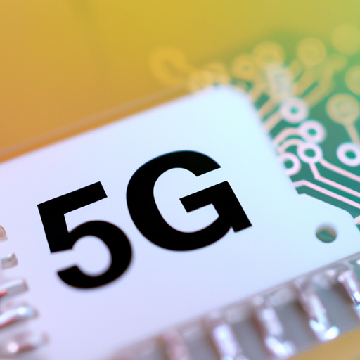
Popular Models of 5G Communication Modules
I. Introduction
As the world becomes increasingly interconnected, the demand for faster and more reliable communication technologies has never been greater. At the forefront of this revolution is 5G technology, which promises to transform how we connect, communicate, and interact with the digital world. Central to this transformation are 5G communication modules, which serve as the backbone for devices and applications that leverage the capabilities of 5G networks. This article will explore the popular models of 5G communication modules, their key features, and their applications, providing a comprehensive overview of this exciting technology.
II. Understanding 5G Technology
A. Evolution from 1G to 5G
The evolution of mobile communication technology has been marked by significant advancements, from the first generation (1G) of analog voice communication to the current fifth generation (5G) that supports a wide array of applications. Each generation has brought improvements in speed, capacity, and functionality, culminating in the high-speed, low-latency capabilities of 5G.
B. Key Features of 5G
5G technology is characterized by several key features that set it apart from its predecessors:
1. **Enhanced Data Rates**: 5G networks can deliver data rates exceeding 10 Gbps, enabling seamless streaming, gaming, and other data-intensive applications.
2. **Low Latency**: With latency as low as 1 millisecond, 5G technology supports real-time applications such as remote surgery and autonomous driving.
3. **Massive Device Connectivity**: 5G can connect up to one million devices per square kilometer, making it ideal for IoT applications and smart cities.
C. Applications of 5G Technology
The potential applications of 5G technology are vast and varied, including:
1. **IoT (Internet of Things)**: 5G enables the interconnection of billions of devices, facilitating smart homes, smart cities, and industrial automation.
2. **Smart Cities**: Enhanced connectivity allows for improved traffic management, energy efficiency, and public safety.
3. **Autonomous Vehicles**: Low latency and high reliability are crucial for the safe operation of self-driving cars.
4. **Enhanced Mobile Broadband**: 5G provides faster and more reliable internet access for mobile users, enhancing the overall user experience.
III. Key Components of 5G Communication Modules
A. Hardware Components
5G communication modules consist of several critical hardware components:
1. **Antennas**: Advanced antenna technologies, such as MIMO (Multiple Input Multiple Output), are essential for maximizing data throughput and coverage.
2. **Chipsets**: The heart of the communication module, chipsets process data and manage communication protocols.
3. **RF Front-End Modules**: These components handle radio frequency signals, ensuring efficient transmission and reception of data.
B. Software Components
In addition to hardware, software components play a vital role in 5G communication modules:
1. **Protocol Stacks**: These software layers manage the communication protocols necessary for data transmission.
2. **Network Management Software**: This software oversees the operation and maintenance of the network, ensuring optimal performance.
C. Integration with Existing Technologies
5G communication modules must integrate seamlessly with existing technologies, including 4G networks, to provide a smooth transition and backward compatibility.
IV. Popular Models of 5G Communication Modules
Several manufacturers have developed notable 5G communication modules, each with unique features and applications. Here are some of the most popular models:
A. Qualcomm Snapdragon X55
1. **Overview**: The Snapdragon X55 is a versatile 5G modem that supports both standalone (SA) and non-standalone (NSA) modes.
2. **Key Features**: It offers peak download speeds of up to 7 Gbps and supports sub-6 GHz and mmWave frequencies.
3. **Applications**: Widely used in smartphones, laptops, and IoT devices, the X55 is known for its efficiency and performance.
B. MediaTek Dimensity 1000
1. **Overview**: The Dimensity 1000 is an integrated 5G SoC (System on Chip) that combines a powerful CPU and GPU with a 5G modem.
2. **Key Features**: It supports dual 5G SIM connectivity and offers impressive AI capabilities for enhanced user experiences.
3. **Applications**: Primarily found in mid-range smartphones, the Dimensity 1000 provides a cost-effective solution for 5G connectivity.
C. Samsung Exynos 5123
1. **Overview**: The Exynos 5123 is Samsung's flagship 5G modem, designed for high-performance devices.
2. **Key Features**: It supports both sub-6 GHz and mmWave frequencies, with download speeds of up to 7.35 Gbps.
3. **Applications**: Used in premium smartphones and tablets, the Exynos 5123 is known for its advanced features and capabilities.
D. Intel XMM 8160
1. **Overview**: The XMM 8160 is Intel's 5G modem, designed for a wide range of devices, including smartphones and laptops.
2. **Key Features**: It supports global 5G bands and offers download speeds of up to 6 Gbps.
3. **Applications**: The XMM 8160 is ideal for mobile computing and IoT applications, providing robust connectivity options.
E. Huawei Balong 5000
1. **Overview**: The Balong 5000 is Huawei's 5G modem, known for its high performance and efficiency.
2. **Key Features**: It supports both SA and NSA modes and offers download speeds of up to 6.5 Gbps.
3. **Applications**: Used in smartphones and home broadband devices, the Balong 5000 is a key player in Huawei's 5G ecosystem.
F. Other Notable Models
1. **NXP Layerscape**: Designed for industrial applications, the Layerscape platform supports 5G connectivity for IoT devices and edge computing.
2. **Sierra Wireless 5G Modules**: These modules are tailored for IoT applications, providing reliable 5G connectivity for various industries.
V. Comparison of 5G Communication Modules
A. Performance Metrics
When comparing 5G communication modules, several performance metrics are essential:
1. **Data Speed**: Different modules offer varying peak download speeds, impacting user experience.
2. **Latency**: Low latency is crucial for applications requiring real-time communication.
3. **Power Consumption**: Efficient power usage is vital for battery-operated devices, especially in IoT applications.
B. Use Cases
The choice of a 5G communication module often depends on the intended use case:
1. **Consumer Electronics**: Smartphones and tablets benefit from high-speed connectivity and low latency.
2. **Industrial Applications**: Modules designed for industrial use prioritize reliability and connectivity in challenging environments.
3. **Automotive Sector**: Automotive applications require modules with ultra-low latency and high reliability for safety-critical functions.
C. Cost Considerations
Cost is a significant factor when selecting a 5G communication module. Manufacturers must balance performance with affordability to meet market demands.
VI. Future Trends in 5G Communication Modules
A. Advancements in Technology
As 5G technology continues to evolve, we can expect advancements in chipsets, antennas, and software that will enhance performance and reduce costs.
B. Integration with AI and Machine Learning
The integration of AI and machine learning into 5G communication modules will enable smarter decision-making and improved network management.
C. The Role of Edge Computing
Edge computing will play a crucial role in 5G, allowing data processing closer to the source and reducing latency for real-time applications.
D. Potential Challenges and Solutions
While 5G technology holds great promise, challenges such as network security, infrastructure costs, and regulatory hurdles must be addressed to ensure successful implementation.
VII. Conclusion
In summary, 5G communication modules are at the heart of the next generation of connectivity, enabling a wide range of applications and transforming industries. With popular models like the Qualcomm Snapdragon X55, MediaTek Dimensity 1000, and Huawei Balong 5000 leading the way, the future of 5G technology looks promising. As advancements continue and new applications emerge, the impact of 5G technology on our daily lives will only grow, paving the way for a more connected and efficient world.
VIII. References
- Academic Journals
- Industry Reports
- Online Resources and Articles
This blog post provides a comprehensive overview of popular models of 5G communication modules, highlighting their features, applications, and the future of 5G technology. As the landscape of communication technology continues to evolve, staying informed about these advancements is essential for businesses and consumers alike.
The Latest Huawei 5G Module Specification Sheet
I. Introduction
A. Overview of 5G Technology
The advent of 5G technology marks a significant leap in telecommunications, promising faster data speeds, lower latency, and the ability to connect a vast number of devices simultaneously. Unlike its predecessors, 5G is designed to support a wide array of applications, from enhanced mobile broadband to the Internet of Things (IoT), paving the way for innovations in various sectors.
B. Importance of 5G Modules in Telecommunications
At the heart of 5G technology are the 5G modules, which serve as the critical components that enable devices to connect to 5G networks. These modules are essential for manufacturers looking to integrate 5G capabilities into their products, whether they are smartphones, IoT devices, or industrial equipment. The specifications of these modules dictate their performance, compatibility, and overall effectiveness in real-world applications.
C. Purpose of the Specification Sheet
This specification sheet aims to provide a comprehensive overview of the latest Huawei 5G module, detailing its features, performance metrics, and potential applications. By understanding these specifications, manufacturers and developers can make informed decisions about integrating Huawei's 5G technology into their products.
II. Background on Huawei
A. Brief History of Huawei in the Telecommunications Industry
Founded in 1987, Huawei has grown from a small telecommunications equipment provider in China to a global leader in the industry. With a focus on innovation and research, Huawei has consistently pushed the boundaries of technology, becoming a key player in the development of mobile networks.
B. Huawei's Role in 5G Development
Huawei has been at the forefront of 5G development, investing heavily in research and development to create cutting-edge solutions. The company has played a pivotal role in standardizing 5G technology and has been involved in numerous trials and deployments worldwide, showcasing its commitment to advancing telecommunications.
C. Overview of Huawei's 5G Product Offerings
Huawei's 5G product portfolio includes a range of solutions, from base stations and routers to 5G modules. These products are designed to meet the diverse needs of various industries, ensuring that customers can leverage the full potential of 5G technology.
III. Key Features of the Latest Huawei 5G Module
A. Technical Specifications
1. Frequency Bands Supported
The latest Huawei 5G module supports a wide range of frequency bands, including sub-6 GHz and mmWave frequencies. This versatility allows it to operate in various network environments, ensuring compatibility with different carriers and regions.
2. Maximum Data Rates
With maximum data rates reaching up to 10 Gbps, the Huawei 5G module is designed to deliver ultra-fast connectivity. This capability is crucial for applications that require high bandwidth, such as video streaming and real-time data processing.
3. Modulation Schemes
The module employs advanced modulation schemes, including 64QAM and 256QAM, to optimize data transmission efficiency. These schemes enhance the module's ability to transmit large amounts of data over the air, improving overall performance.
B. Form Factor and Design
1. Size and Weight
The Huawei 5G module features a compact design, making it suitable for integration into various devices without adding significant bulk. Its lightweight construction ensures that it can be easily incorporated into mobile devices, IoT sensors, and other applications.
2. Interface Options
The module offers multiple interface options, including PCIe, USB, and UART, providing flexibility for manufacturers. This variety allows for seamless integration into existing systems and facilitates easy communication with other components.
C. Power Consumption
1. Operating Voltage
Designed for efficiency, the Huawei 5G module operates at a low voltage, minimizing power consumption while maintaining high performance. This feature is particularly beneficial for battery-powered devices, extending their operational lifespan.
2. Power-Saving Features
The module incorporates advanced power-saving features, such as dynamic power scaling and sleep modes, which help reduce energy consumption during periods of inactivity. These features are essential for IoT applications, where devices may need to operate for extended periods on limited power sources.
IV. Performance Metrics
A. Throughput and Latency
The Huawei 5G module delivers impressive throughput rates, ensuring that data can be transmitted quickly and efficiently. With latency as low as 1 millisecond, the module is well-suited for applications that require real-time communication, such as remote surgery and autonomous driving.
B. Reliability and Stability
Reliability is a critical factor in telecommunications, and the Huawei 5G module is designed to provide stable connections even in challenging environments. Its robust architecture ensures consistent performance, reducing the likelihood of dropped connections or service interruptions.
C. Coverage and Range
The module's ability to support both sub-6 GHz and mmWave frequencies enhances its coverage and range. This flexibility allows it to provide reliable connectivity in urban areas with high device density as well as in rural regions where signal strength may be weaker.
V. Use Cases and Applications
A. Industrial IoT
The Huawei 5G module is ideal for industrial IoT applications, enabling real-time monitoring and control of machinery and equipment. Its high data rates and low latency facilitate seamless communication between devices, improving operational efficiency and reducing downtime.
B. Smart Cities
In the context of smart cities, the module can support a wide range of applications, from traffic management systems to smart lighting. By connecting various devices and sensors, it enables city planners to optimize resources and enhance the quality of life for residents.
C. Autonomous Vehicles
The low latency and high reliability of the Huawei 5G module make it a perfect fit for autonomous vehicles. It allows for real-time data exchange between vehicles and infrastructure, enhancing safety and enabling advanced features such as vehicle-to-everything (V2X) communication.
D. Enhanced Mobile Broadband
For consumers, the Huawei 5G module provides enhanced mobile broadband experiences, enabling faster downloads, smoother streaming, and improved online gaming. This capability is essential as more users rely on mobile devices for their daily activities.
VI. Comparison with Competitors
A. Overview of Other Leading 5G Module Manufacturers
The 5G module market is competitive, with several key players, including Qualcomm, Intel, and Samsung. Each manufacturer offers unique features and capabilities, catering to different segments of the market.
B. Key Differentiators of Huawei's 5G Module
Huawei's 5G module stands out due to its comprehensive support for multiple frequency bands, impressive data rates, and advanced power-saving features. Additionally, Huawei's extensive experience in telecommunications gives it a competitive edge in terms of reliability and performance.
C. Market Positioning and Advantages
Huawei's strong market positioning is bolstered by its commitment to research and development, allowing it to stay ahead of trends and technological advancements. This focus ensures that its 5G modules remain relevant and competitive in a rapidly evolving landscape.
VII. Future Developments
A. Upcoming Features and Enhancements
Huawei is continuously working on enhancing its 5G modules, with upcoming features expected to include improved AI capabilities for network optimization and enhanced security measures to protect against emerging threats.
B. Huawei's Roadmap for 5G Technology
The company's roadmap for 5G technology includes plans for expanding its product offerings and exploring new applications in sectors such as healthcare, transportation, and entertainment. This forward-thinking approach positions Huawei as a leader in the 5G space.
C. Potential Impact on the Telecommunications Landscape
As Huawei continues to innovate, its 5G modules are likely to play a significant role in shaping the future of telecommunications. The widespread adoption of 5G technology will enable new business models and services, transforming industries and enhancing connectivity worldwide.
VIII. Conclusion
A. Summary of Key Points
The latest Huawei 5G module represents a significant advancement in telecommunications technology, offering impressive specifications, performance metrics, and a wide range of applications. Its versatility and efficiency make it a valuable asset for manufacturers and developers looking to leverage 5G capabilities.
B. The Significance of Huawei's 5G Module in the Industry
Huawei's contributions to 5G technology are crucial for the industry's evolution, providing the tools necessary for businesses to innovate and thrive in a connected world. The company's commitment to research and development ensures that its products remain at the forefront of technological advancements.
C. Final Thoughts on the Future of 5G Technology
As 5G technology continues to evolve, the potential for new applications and services is limitless. Huawei's latest 5G module is poised to play a pivotal role in this transformation, enabling a future where connectivity is faster, more reliable, and more accessible than ever before.
IX. References
A. List of Sources and Further Reading Materials
1. Huawei Official Website
2. Industry Reports on 5G Technology
3. Telecommunications Journals and Publications
B. Links to Huawei's Official Documentation and Specifications
- [Huawei 5G Module Specifications](https://www.huawei.com/en/5g)
- [5G Technology Overview](https://www.huawei.com/en/technology/5g)
This blog post provides a detailed overview of the latest Huawei 5G module specification sheet, highlighting its features, performance, and potential applications in various industries. By understanding these aspects, readers can appreciate the significance of Huawei's contributions to the 5G landscape.
What is the Mainstream 5G Radio Frequency Module Production Process?
I. Introduction
As the world becomes increasingly interconnected, the demand for faster and more reliable communication technologies has surged. At the forefront of this revolution is 5G technology, which promises to transform how we communicate, work, and live. Central to the functionality of 5G networks are 5G Radio Frequency (RF) modules, which play a crucial role in transmitting and receiving data. This blog post will explore the production process of these essential components, shedding light on the intricate steps involved in bringing 5G RF modules to life.
II. Understanding 5G Technology
A. Brief History of Mobile Communication Technologies
The evolution of mobile communication technologies has been marked by significant milestones, from the first generation (1G) of analog voice communication to the current 5G networks. Each generation has brought improvements in speed, capacity, and functionality, paving the way for the advanced capabilities we see today.
B. Key Features of 5G Technology
5G technology is characterized by several key features that set it apart from its predecessors:
1. **Enhanced Data Rates**: 5G networks can deliver data rates exceeding 10 Gbps, enabling seamless streaming, gaming, and real-time applications.
2. **Reduced Latency**: With latency as low as 1 millisecond, 5G allows for instantaneous communication, which is critical for applications like autonomous vehicles and remote surgery.
3. **Increased Connectivity**: 5G can support a massive number of devices per square kilometer, making it ideal for the Internet of Things (IoT) and smart city applications.
C. Role of Radio Frequency Modules in 5G
Radio Frequency modules are integral to the operation of 5G networks. They facilitate the transmission and reception of radio signals, converting digital data into radio waves and vice versa. Without these modules, the high-speed and low-latency capabilities of 5G would not be possible.
III. Components of 5G Radio Frequency Modules
5G RF modules consist of several critical components:
A. Transmitters and Receivers
These components are responsible for sending and receiving signals. Transmitters convert electrical signals into radio waves, while receivers perform the opposite function.
B. Antennas
Antennas are essential for radiating and capturing radio waves. In 5G modules, advanced antenna technologies, such as Massive MIMO (Multiple Input Multiple Output), are employed to enhance performance.
C. Power Amplifiers
Power amplifiers boost the strength of the transmitted signals, ensuring they can travel long distances without significant loss of quality.
D. Filters and Duplexers
Filters eliminate unwanted frequencies, while duplexers allow simultaneous transmission and reception of signals, optimizing the use of the available spectrum.
E. Integrated Circuits (ICs)
ICs are the brain of the RF module, processing signals and controlling various functions within the module.
IV. Overview of the Production Process
The production of 5G RF modules involves several key stages, each critical to ensuring the final product meets the required specifications.
A. Research and Development (R&D)
1. Design and Prototyping
The production process begins with R&D, where engineers design the RF module. This phase includes creating prototypes to test various configurations and functionalities.
2. Simulation and Testing
Before moving to production, simulations are conducted to predict the module's performance under different conditions. This step helps identify potential issues early in the process.
B. Material Selection
1. Types of Materials Used
The choice of materials is crucial in RF module production. Common materials include silicon for ICs, various metals for antennas, and specialized ceramics for filters.
2. Importance of Material Properties
The properties of these materials, such as conductivity, thermal stability, and dielectric constant, significantly impact the module's performance.
C. Manufacturing Techniques
1. Semiconductor Fabrication
The fabrication of semiconductor components involves processes like photolithography and etching to create intricate patterns on silicon wafers.
2. Surface Mount Technology (SMT)
SMT is used to attach components to the surface of PCBs (Printed Circuit Boards), allowing for compact designs and efficient manufacturing.
3. Assembly Processes
Once the components are fabricated, they are assembled into the final RF module. This process may involve manual and automated techniques to ensure precision.
D. Quality Control and Testing
1. In-Process Quality Checks
Quality control is integrated throughout the production process, with regular checks to ensure components meet specifications.
2. Final Testing Procedures
After assembly, the modules undergo rigorous testing to verify their performance, including electrical testing and environmental testing to ensure reliability under various conditions.
V. Detailed Steps in the Production Process
A. Design Phase
1. Circuit Design
The design phase involves creating detailed circuit diagrams that outline how each component will interact within the module.
2. Layout Design
Layout design translates the circuit diagrams into physical layouts for the PCB, ensuring optimal placement of components for performance and manufacturability.
B. Fabrication Phase
1. Wafer Fabrication
In this phase, silicon wafers are processed to create the semiconductor components. This involves multiple steps, including doping, oxidation, and metallization.
2. Die Preparation
Once the wafers are fabricated, individual dies are cut from the wafer and prepared for assembly.
C. Assembly Phase
1. Component Placement
Components are placed onto the PCB using automated pick-and-place machines, ensuring accuracy and speed.
2. Soldering Techniques
Soldering techniques, such as reflow soldering, are employed to secure components to the PCB, creating reliable electrical connections.
D. Testing Phase
1. Electrical Testing
Electrical testing verifies that the module functions correctly, checking parameters like signal strength and frequency response.
2. Environmental Testing
Environmental testing assesses the module's performance under various conditions, including temperature extremes and humidity, to ensure reliability in real-world applications.
VI. Challenges in 5G Radio Frequency Module Production
A. Technological Challenges
1. Miniaturization
As devices become smaller, the challenge of miniaturizing RF modules while maintaining performance becomes increasingly complex.
2. Heat Management
5G modules generate significant heat, necessitating advanced cooling solutions to prevent overheating and ensure reliability.
B. Supply Chain Issues
1. Material Shortages
The global demand for electronic components has led to material shortages, impacting production timelines and costs.
2. Global Supply Chain Disruptions
Recent global events have highlighted vulnerabilities in supply chains, affecting the availability of critical components.
C. Regulatory Compliance
1. Standards and Certifications
Manufacturers must navigate a complex landscape of standards and certifications to ensure their products meet regulatory requirements.
2. Environmental Regulations
Increasingly stringent environmental regulations require manufacturers to adopt sustainable practices in their production processes.
VII. Future Trends in 5G Radio Frequency Module Production
A. Advancements in Materials and Technologies
The future of 5G RF module production will likely see the development of new materials and technologies that enhance performance and reduce costs.
B. The Role of Artificial Intelligence and Automation
AI and automation are expected to play a significant role in optimizing production processes, improving efficiency, and reducing human error.
C. Sustainability in Production Processes
As environmental concerns grow, manufacturers will increasingly focus on sustainable practices, including recycling materials and reducing waste.
VIII. Conclusion
5G Radio Frequency modules are vital components that enable the high-speed, low-latency communication that defines 5G technology. Understanding the production process—from design and material selection to manufacturing and testing—provides insight into the complexity and precision required to bring these modules to market. As technology continues to evolve, the future of 5G RF module production promises exciting advancements that will further enhance our communication capabilities.
IX. References
- Academic Journals
- Industry Reports
- Relevant Books and Articles
This blog post provides a comprehensive overview of the mainstream production process of 5G radio frequency modules, highlighting the intricate steps and challenges involved in creating these essential components of modern communication technology.
Mainstream 5G Optical Module Concept Stock Product Series Parameters
I. Introduction
A. Overview of 5G Technology
The advent of 5G technology marks a significant leap in telecommunications, promising faster data speeds, lower latency, and the ability to connect a vast number of devices simultaneously. As the backbone of modern communication, 5G is set to revolutionize industries, enhance user experiences, and enable innovations such as smart cities, autonomous vehicles, and the Internet of Things (IoT).
B. Purpose of the Document
This blog post aims to provide an in-depth understanding of mainstream 5G optical module concepts and outline the parameters of various product series. By exploring the role of optical modules in 5G networks, we can appreciate their significance in achieving the ambitious goals set by this transformative technology.
II. Understanding Optical Modules
A. Definition and Function of Optical Modules
Optical modules are essential components in optical communication systems, facilitating the transmission of data over fiber optic cables. They convert electrical signals into optical signals and vice versa, enabling high-speed data transfer across long distances.
1. Explanation of Optical Communication
Optical communication utilizes light to transmit information, offering several advantages over traditional copper-based systems, including higher bandwidth, longer transmission distances, and immunity to electromagnetic interference.
2. Components of Optical Modules
An optical module typically consists of a transmitter, receiver, and various supporting components such as lasers, photodetectors, and signal processing units. These components work together to ensure efficient data transmission and reception.
B. Types of Optical Modules
Optical modules can be categorized into several types, each serving specific functions within a network.
1. Transceivers
Transceivers are the most common type of optical module, combining both transmission and reception capabilities. They are used in various applications, from data centers to telecommunications networks.
2. Optical Amplifiers
Optical amplifiers boost the strength of optical signals, allowing them to travel longer distances without degradation. They are crucial in long-haul communication systems.
3. Optical Switches
Optical switches enable the routing of optical signals between different paths in a network, enhancing flexibility and efficiency in data transmission.
III. The Role of Optical Modules in 5G Networks
Optical modules play a pivotal role in the performance and efficiency of 5G networks.
A. Enhancing Data Transmission Speeds
With the demand for high-speed data transmission skyrocketing, optical modules are designed to support data rates of 25G, 100G, and even 400G. This capability is essential for delivering the ultra-fast internet speeds promised by 5G technology.
B. Supporting Low Latency Communication
5G networks aim to achieve latency as low as one millisecond, a feat made possible by the rapid data transfer capabilities of optical modules. This low latency is critical for applications such as real-time gaming, remote surgery, and autonomous driving.
C. Enabling Massive Device Connectivity
The ability to connect millions of devices simultaneously is a hallmark of 5G technology. Optical modules facilitate this connectivity by providing the necessary bandwidth and reliability to support a dense network of devices.
D. Importance in Backhaul and Fronthaul Networks
In 5G architecture, optical modules are integral to both backhaul and fronthaul networks. Backhaul refers to the connection between the core network and base stations, while fronthaul connects the base stations to the radio units. Optical modules ensure efficient data transfer in both scenarios, supporting the overall network performance.
IV. Mainstream 5G Optical Module Concepts
A. Overview of Mainstream Concepts
The design and implementation of optical modules in 5G networks involve several mainstream concepts.
1. Single-Mode vs. Multi-Mode Fibers
Single-mode fibers are designed for long-distance communication, allowing only one mode of light to propagate. In contrast, multi-mode fibers support multiple light modes, making them suitable for shorter distances. The choice between these fiber types depends on the specific requirements of the network.
2. Wavelength Division Multiplexing (WDM)
Wavelength Division Multiplexing is a technology that enables multiple optical signals to be transmitted simultaneously over a single fiber by using different wavelengths (or colors) of light. This technique significantly increases the capacity of optical networks, making it a vital component of 5G infrastructure.
B. Key Technologies in 5G Optical Modules
Several key technologies underpin the functionality of 5G optical modules.
1. Coherent Optical Technology
Coherent optical technology allows for the transmission of data at higher speeds and longer distances by utilizing advanced modulation formats and digital signal processing. This technology is essential for meeting the demands of 5G networks.
2. Digital Signal Processing (DSP)
Digital signal processing enhances the performance of optical modules by improving signal quality and reducing errors. DSP techniques are crucial for managing the complexities of high-speed data transmission.
3. Photonic Integration
Photonic integration involves combining multiple optical components onto a single chip, reducing size and power consumption while increasing performance. This technology is becoming increasingly important in the development of compact and efficient optical modules for 5G.
V. Product Series Parameters
A. Performance Metrics
When evaluating optical modules for 5G applications, several performance metrics are critical.
1. Data Rates
Optical modules are available in various data rates, including 25G, 100G, and 400G. The choice of data rate depends on the specific application and network requirements.
2. Transmission Distance
The transmission distance of optical modules varies based on the type of fiber used and the technology employed. Long-haul modules can transmit data over hundreds of kilometers, while short-range modules are designed for data center applications.
3. Latency Specifications
Latency is a crucial factor in 5G networks, and optical modules must meet stringent latency requirements to ensure optimal performance.
B. Form Factors
The form factor of optical modules refers to their physical design and compatibility with existing infrastructure.
1. SFP, SFP+, QSFP, QSFP28, etc.
Various form factors, such as SFP (Small Form-factor Pluggable), SFP+, QSFP (Quad Small Form-factor Pluggable), and QSFP28, are available to accommodate different network configurations and requirements.
2. Compatibility with Existing Infrastructure
Ensuring compatibility with existing network infrastructure is essential for seamless integration and deployment of optical modules.
C. Power Consumption and Efficiency
Power consumption is a critical consideration in the design of optical modules, as energy efficiency directly impacts operational costs and environmental sustainability.
D. Environmental Considerations
1. Operating Temperature Ranges
Optical modules must operate effectively within specific temperature ranges to ensure reliability in various environments.
2. Compliance with Industry Standards
Compliance with industry standards is essential for ensuring the quality and reliability of optical modules in 5G networks.
VI. Market Trends and Innovations
A. Current Market Landscape for 5G Optical Modules
The market for 5G optical modules is rapidly evolving, driven by the increasing demand for high-speed connectivity and the expansion of 5G networks worldwide.
B. Emerging Technologies and Their Impact
1. AI and Machine Learning in Optical Networks
Artificial intelligence and machine learning are being integrated into optical networks to optimize performance, enhance security, and improve network management.
2. Advancements in Photonic Materials
Research into new photonic materials is paving the way for more efficient and compact optical modules, further enhancing the capabilities of 5G networks.
C. Future Outlook for 5G Optical Modules
The future of 5G optical modules looks promising, with ongoing innovations and advancements expected to drive further improvements in performance, efficiency, and integration.
VII. Conclusion
A. Recap of the Importance of Optical Modules in 5G
Optical modules are a cornerstone of 5G technology, enabling high-speed data transmission, low latency communication, and massive device connectivity. Their role in backhaul and fronthaul networks is critical for the overall performance of 5G infrastructure.
B. Final Thoughts on the Evolution of Optical Module Technology
As the telecommunications landscape continues to evolve, optical module technology will play an increasingly vital role in meeting the demands of next-generation networks.
C. Call to Action for Stakeholders in the Telecommunications Industry
Stakeholders in the telecommunications industry must stay informed about the latest developments in optical module technology to leverage its potential fully and drive the successful deployment of 5G networks.
VIII. References
A comprehensive list of academic papers, industry reports, and relevant resources for further reading will be provided to support the information presented in this blog post.
In conclusion, understanding the parameters and concepts surrounding mainstream 5G optical modules is essential for anyone involved in the telecommunications industry. As we move towards a more connected future, the importance of these technologies will only continue to grow.
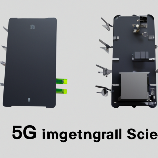
Mainstream 5G Communication Module Product Series Parameters
I. Introduction
A. Overview of 5G Technology
5G, the fifth generation of mobile network technology, represents a significant leap forward in wireless communication. It is designed to provide faster speeds, lower latency, and greater capacity than its predecessors. The evolution from earlier generations—2G, 3G, and 4G—has paved the way for a more connected world, enabling a plethora of applications that were previously unimaginable. While 2G introduced basic voice services, 3G brought mobile internet, and 4G enhanced data speeds, 5G is set to revolutionize connectivity by supporting a vast array of devices and applications, from smart cities to autonomous vehicles.
B. Importance of 5G Communication Modules
At the heart of 5G technology are communication modules, which play a crucial role in enabling devices to connect to 5G networks. These modules are essential for various industries, including telecommunications, automotive, healthcare, and manufacturing. They facilitate high-speed data transfer, real-time communication, and seamless connectivity, making them indispensable for the implementation of 5G technology across different sectors.
II. Key Features of 5G Communication Modules
A. Speed and Bandwidth
One of the most significant advantages of 5G communication modules is their speed. 5G networks can theoretically achieve speeds of up to 10 Gbps, which is up to 100 times faster than 4G. This increase in speed has profound implications for data-intensive applications such as virtual reality (VR), augmented reality (AR), and high-definition video streaming. With 5G, users can download large files in seconds and enjoy uninterrupted streaming experiences.
B. Latency
Latency, the time it takes for data to travel from the source to the destination, is another critical feature of 5G communication modules. 5G technology aims to reduce latency to as low as 1 millisecond, compared to 30-50 milliseconds for 4G. This low latency is vital for applications that require real-time feedback, such as remote surgery, autonomous driving, and industrial automation. The ability to transmit data almost instantaneously opens up new possibilities for innovation and efficiency.
C. Connectivity and Capacity
5G communication modules also enhance connectivity and capacity, allowing networks to support a significantly higher number of devices per square kilometer. This capability is particularly important for the Internet of Things (IoT) and smart city initiatives, where millions of devices need to communicate simultaneously. With 5G, cities can implement smart traffic management systems, connected public transportation, and efficient energy management, leading to improved urban living.
III. Types of 5G Communication Modules
A. Sub-6 GHz Modules
Sub-6 GHz modules operate within the frequency range below 6 GHz and are characterized by their ability to provide broad coverage and reliable connectivity. These modules are ideal for urban and suburban environments, where they can penetrate buildings and obstacles effectively. Use cases include mobile broadband, fixed wireless access, and IoT applications.
B. mmWave Modules
Millimeter-wave (mmWave) modules operate at higher frequencies, typically above 24 GHz. They offer significantly higher data rates and capacity but have a shorter range and limited penetration through obstacles. mmWave is best suited for dense urban areas and high-traffic environments, such as stadiums and concert venues, where large amounts of data need to be transmitted quickly.
C. Dual-Band Modules
Dual-band modules combine the capabilities of both sub-6 GHz and mmWave technologies, providing versatility in various environments. These modules can switch between frequency bands based on the network conditions, ensuring optimal performance. They are particularly useful for applications that require both wide coverage and high-speed data transfer, such as smart factories and connected vehicles.
IV. Technical Parameters of 5G Communication Modules
A. Frequency Bands
5G communication modules operate across various frequency bands, which are allocated differently in regions such as the US, EU, and Asia. Understanding these frequency allocations is crucial for manufacturers and developers to ensure compatibility with local networks. For instance, the US has allocated bands like n77 and n78 for 5G, while Europe has its own set of bands, leading to variations in module design and functionality.
B. Modulation Techniques
Modulation techniques play a vital role in the performance and efficiency of 5G communication modules. Orthogonal Frequency Division Multiplexing (OFDM) is a key technique used in 5G, allowing for efficient data transmission over multiple channels. This technique enhances spectral efficiency and reduces interference, making it ideal for high-capacity networks.
C. Power Consumption
Energy efficiency is a critical consideration for 5G communication modules, especially as the number of connected devices continues to grow. Compared to previous generation modules, 5G modules are designed to consume less power while delivering higher performance. This focus on energy efficiency not only reduces operational costs but also supports sustainability initiatives.
V. Integration and Compatibility
A. Hardware Integration
Integrating 5G communication modules with existing systems can present challenges, particularly for legacy infrastructure. Ensuring compatibility with various hardware components is essential for seamless operation. Manufacturers must consider factors such as form factor, interface standards, and connectivity options when designing 5G modules.
B. Software and Firmware
Software and firmware play a crucial role in the functionality of 5G communication modules. Regular software updates and support are necessary to maintain performance and security. Additionally, the availability of Application Programming Interfaces (APIs) and Software Development Kits (SDKs) facilitates the development of applications that leverage 5G capabilities, enabling developers to create innovative solutions.
VI. Market Trends and Future Developments
A. Current Market Landscape
The 5G module market is rapidly evolving, with key players such as Qualcomm, Intel, and Huawei leading the charge. As demand for 5G connectivity grows, market share and growth projections indicate a robust future for 5G communication modules. Analysts predict that the global 5G module market will reach billions of dollars in the coming years, driven by increased adoption across various industries.
B. Future Innovations
Emerging technologies such as artificial intelligence (AI) and edge computing are set to shape the future of 5G communication modules. AI can enhance network management and optimization, while edge computing allows for data processing closer to the source, reducing latency and improving efficiency. As these technologies continue to develop, they will further enhance the capabilities of 5G modules and expand their applications.
VII. Conclusion
A. Summary of Key Points
In summary, 5G communication modules are a cornerstone of the fifth generation of mobile technology, offering unprecedented speed, low latency, and enhanced connectivity. With various types of modules available, including sub-6 GHz, mmWave, and dual-band options, industries can choose the best solutions for their specific needs.
B. The Future of 5G Communication Modules
The long-term implications of 5G communication modules are profound, with the potential to transform industries and improve the lives of consumers. As 5G technology continues to evolve, it will play a pivotal role in shaping the digital landscape, driving innovation, and enabling a more connected world. The future of 5G communication modules is bright, and their impact will be felt across all sectors of society.
VIII. References
1. 3GPP. (2023). "Technical Specifications for 5G."
2. GSMA. (2023). "The Mobile Economy 2023."
3. Qualcomm. (2023). "5G Technology Overview."
4. Ericsson. (2023). "Ericsson Mobility Report."
5. International Telecommunication Union (ITU). (2023). "5G: The Next Generation of Mobile Networks."
This blog post provides a comprehensive overview of the parameters of mainstream 5G communication module products, highlighting their significance, features, types, technical specifications, and future trends. As 5G technology continues to advance, understanding these modules will be essential for leveraging their full potential in various applications.
Important Product Categories of 5G Wireless Modules
I. Introduction
As we stand on the brink of a new era in wireless communication, 5G technology is set to revolutionize the way we connect, communicate, and interact with the world around us. At the heart of this transformation are 5G wireless modules, which serve as the essential building blocks for a wide range of applications. This article aims to explore the important product categories of 5G wireless modules, highlighting their significance in various sectors and the potential they hold for the future.
II. Understanding 5G Wireless Modules
A. What are Wireless Modules?
Wireless modules are compact, integrated circuits that enable devices to connect to wireless networks. They typically include a radio transceiver, a microcontroller, and various interfaces for communication with other components. In the context of 5G, these modules are designed to leverage the advanced capabilities of the fifth generation of mobile networks, providing faster data rates, lower latency, and improved connectivity.
B. The Role of 5G in Wireless Communication
5G technology represents a significant leap forward from its predecessors, offering enhanced speed, capacity, and reliability. It is designed to support a vast array of devices and applications, from smartphones to industrial machinery, making it a cornerstone of the Internet of Things (IoT) and smart technologies.
C. Key Features of 5G Wireless Modules
1. **Speed and Bandwidth**: 5G wireless modules can deliver data rates exceeding 10 Gbps, enabling high-definition video streaming, real-time gaming, and other bandwidth-intensive applications.
2. **Latency**: With latency as low as 1 millisecond, 5G modules facilitate instantaneous communication, which is crucial for applications like autonomous driving and remote surgery.
3. **Connectivity and Range**: 5G technology supports a massive number of connected devices, making it ideal for smart cities and industrial IoT applications.
4. **Energy Efficiency**: 5G modules are designed to consume less power, extending the battery life of connected devices and reducing operational costs.
III. Major Product Categories of 5G Wireless Modules
A. Consumer Electronics
The consumer electronics sector is one of the most visible beneficiaries of 5G technology.
1. **Smartphones**: The introduction of 5G-enabled smartphones has transformed mobile communication, allowing users to experience faster downloads, smoother streaming, and enhanced gaming experiences.
2. **Tablets**: 5G tablets provide users with the ability to work and play on-the-go, offering high-speed internet access without the need for Wi-Fi.
3. **Laptops**: With 5G modules integrated into laptops, users can enjoy seamless connectivity, enabling remote work and online collaboration.
4. **Wearable Devices**: Smartwatches and fitness trackers equipped with 5G modules can provide real-time health monitoring and communication, enhancing user experience and functionality.
B. Industrial IoT (IIoT)
The industrial sector is rapidly adopting 5G technology to enhance operational efficiency and productivity.
1. **Smart Factories**: 5G wireless modules enable real-time data exchange between machines, facilitating automation and predictive maintenance.
2. **Remote Monitoring Systems**: Industries can monitor equipment and processes remotely, reducing downtime and improving safety.
3. **Asset Tracking Solutions**: 5G technology allows for precise tracking of assets in real-time, optimizing supply chain management and logistics.
C. Automotive Applications
The automotive industry is undergoing a significant transformation with the integration of 5G technology.
1. **Connected Vehicles**: 5G modules enable vehicles to communicate with each other and with infrastructure, enhancing safety and traffic management.
2. **Autonomous Driving Systems**: Low latency and high reliability are critical for autonomous vehicles, making 5G an essential component of their operation.
3. **Vehicle-to-Everything (V2X) Communication**: This technology allows vehicles to communicate with other vehicles, pedestrians, and traffic signals, improving overall road safety.
D. Smart Cities
5G technology plays a crucial role in the development of smart cities, enhancing urban living through connectivity.
1. **Smart Traffic Management**: 5G modules can facilitate real-time traffic monitoring and management, reducing congestion and improving public transport efficiency.
2. **Public Safety and Surveillance**: Enhanced connectivity allows for better surveillance systems and emergency response coordination.
3. **Environmental Monitoring**: 5G technology enables the deployment of sensors to monitor air quality, noise levels, and other environmental factors, contributing to sustainable urban development.
E. Healthcare Solutions
The healthcare sector is leveraging 5G technology to improve patient care and operational efficiency.
1. **Telemedicine**: 5G modules enable high-quality video consultations, making healthcare more accessible to patients in remote areas.
2. **Remote Patient Monitoring**: Healthcare providers can monitor patients' vital signs in real-time, allowing for timely interventions and better management of chronic conditions.
3. **Medical Device Connectivity**: 5G technology facilitates seamless communication between medical devices, improving data accuracy and patient outcomes.
F. Retail and E-commerce
The retail sector is also experiencing a transformation due to 5G technology.
1. **Smart Retail Solutions**: Retailers can use 5G modules to enhance customer experiences through personalized marketing and real-time inventory management.
2. **Inventory Management Systems**: 5G technology allows for real-time tracking of inventory, reducing stockouts and improving supply chain efficiency.
3. **Enhanced Customer Experience**: With faster connectivity, retailers can offer immersive shopping experiences, such as augmented reality (AR) applications.
G. Telecommunications Infrastructure
Telecommunications companies are investing heavily in 5G infrastructure to support the growing demand for connectivity.
1. **Base Stations**: 5G wireless modules are essential for the deployment of base stations, which provide coverage and capacity for mobile networks.
2. **Network Slicing**: This technology allows operators to create virtual networks tailored to specific applications, optimizing resource allocation.
3. **Edge Computing Solutions**: 5G modules enable edge computing, bringing data processing closer to the source and reducing latency for critical applications.
IV. Key Players in the 5G Wireless Module Market
A. Overview of Major Manufacturers
The 5G wireless module market is dominated by several key players, including Qualcomm, Intel, and Ericsson, who are leading the charge in developing innovative solutions.
B. Emerging Startups and Innovators
In addition to established companies, numerous startups are emerging in the 5G space, focusing on niche applications and innovative technologies.
C. Collaborations and Partnerships
Collaborations between technology companies, telecommunications providers, and research institutions are driving advancements in 5G technology, fostering innovation and accelerating market growth.
V. Challenges and Considerations
A. Technical Challenges
1. **Integration with Existing Networks**: Transitioning to 5G requires significant upgrades to existing infrastructure, posing challenges for operators.
2. **Security Concerns**: As connectivity increases, so do security risks, necessitating robust measures to protect data and networks.
B. Regulatory and Compliance Issues
Navigating the regulatory landscape is crucial for the successful deployment of 5G technology, as compliance with local laws and standards is essential.
C. Market Adoption and Consumer Awareness
Raising awareness about the benefits of 5G technology is vital for driving adoption among consumers and businesses alike.
VI. Future Trends in 5G Wireless Modules
A. Advancements in Technology
As technology continues to evolve, we can expect further enhancements in 5G wireless modules, including improved performance and reduced costs.
B. Potential New Applications
The versatility of 5G technology opens the door to new applications across various sectors, from smart agriculture to advanced manufacturing.
C. The Role of AI and Machine Learning
Integrating AI and machine learning with 5G technology will enable smarter decision-making and automation, enhancing the capabilities of connected devices.
VII. Conclusion
In conclusion, 5G wireless modules are poised to play a pivotal role in shaping the future of connectivity and communication. From consumer electronics to industrial applications, the impact of 5G technology is far-reaching and transformative. As stakeholders in the industry continue to innovate and collaborate, the potential for new applications and advancements is limitless. It is essential for businesses, governments, and consumers to embrace this technology and harness its capabilities for a more connected and efficient world.
VIII. References
A comprehensive list of studies, articles, and reports will be provided to support the information presented in this article, along with additional resources for further reading on 5G technology and its applications.
基本
文件
流程
错误
SQL
调试
- 请求信息 : 2025-05-11 17:37:02 HTTP/1.1 GET : http://szshuoshi.com/en/news
- 运行时间 : 0.077018s [ 吞吐率:12.98req/s ] 内存消耗:1,579.49kb 文件加载:201
- 查询信息 : 0 queries
- 缓存信息 : 2 reads,0 writes
- 会话信息 : SESSION_ID=9b52a1e4fc309d5dd0d17e46da7bb0ed
- CONNECT:[ UseTime:0.002525s ] mysql:host=localhost;port=3306;dbname=szshuoshi_com;charset=utf8mb4
- SHOW FULL COLUMNS FROM `moban_site` [ RunTime:0.003880s ]
- SELECT * FROM `moban_site` WHERE `lang` = 'en' LIMIT 1 [ RunTime:0.000992s ]
- SHOW FULL COLUMNS FROM `moban_columns` [ RunTime:0.002629s ]
- SELECT * FROM `moban_columns` WHERE `state` = 1 AND `lang` = 'en' ORDER BY `sort` ASC [ RunTime:0.001021s ]
- SHOW FULL COLUMNS FROM `moban_news` [ RunTime:0.002577s ]
- SELECT * FROM `moban_news` WHERE `lang` = 'en' AND `state` = 1 LIMIT 1 [ RunTime:0.001084s ]
- SHOW FULL COLUMNS FROM `moban_news_category` [ RunTime:0.002273s ]
- SELECT * FROM `moban_news_category` WHERE `lang` = 'en' ORDER BY `id` ASC [ RunTime:0.000910s ]
- SHOW FULL COLUMNS FROM `moban_single_page` [ RunTime:0.002437s ]
- SELECT * FROM `moban_single_page` WHERE `id` IN (0,28,34,73) AND `state` = 1 AND `lang` = 'en' [ RunTime:0.000962s ]
- SELECT * FROM `moban_single_page` WHERE `id` IN (0,2,68) AND `state` = 1 AND `lang` = 'en' [ RunTime:0.000568s ]
- SHOW FULL COLUMNS FROM `moban_link` [ RunTime:0.002359s ]
- SELECT * FROM `moban_link` WHERE `state` = 1 ORDER BY `sort` ASC [ RunTime:0.000548s ]
- SELECT COUNT(*) AS think_count FROM `moban_news` WHERE `state` = 1 AND `lang` = 'en' AND `is_draft` = 0 LIMIT 1 [ RunTime:0.000621s ]
- SELECT * FROM `moban_news` WHERE `state` = 1 AND `lang` = 'en' AND `is_draft` = 0 ORDER BY `sort` DESC,`id` DESC LIMIT 0,25 [ RunTime:0.001837s ]
- SELECT * FROM `moban_columns` WHERE `lang` = 'en' AND `link` = '/news' LIMIT 1 [ RunTime:0.000780s ]

0.093506s


